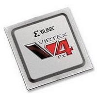
XC4VFX20-10FFG672C Xilinx Inc, XC4VFX20-10FFG672C Datasheet - Page 83

XC4VFX20-10FFG672C
Manufacturer Part Number
XC4VFX20-10FFG672C
Description
IC FPGA VIRTEX-4 FX 20K 672-FBGA
Manufacturer
Xilinx Inc
Series
Virtex™-4r
Datasheets
1.XC4VFX12-10FFG668C.pdf
(58 pages)
2.XC4VFX12-10FFG668C.pdf
(9 pages)
3.XC4VFX12-10FFG668C.pdf
(406 pages)
Specifications of XC4VFX20-10FFG672C
Total Ram Bits
1253376
Number Of Logic Elements/cells
19224
Number Of Labs/clbs
2136
Number Of I /o
320
Voltage - Supply
1.14 V ~ 1.26 V
Mounting Type
Surface Mount
Operating Temperature
0°C ~ 85°C
Package / Case
672-BBGA, FCBGA
No. Of Logic Blocks
19224
No. Of Macrocells
19224
No. Of Speed Grades
10
No. Of I/o's
320
Clock Management
DCM
I/o Supply Voltage
3.45V
Lead Free Status / RoHS Status
Lead free / RoHS Compliant
For Use With
HW-V4-ML405-UNI-G - EVALUATION PLATFORM VIRTEX-4
Number Of Gates
-
Lead Free Status / RoHS Status
Lead free / RoHS Compliant, Lead free / RoHS Compliant
Available stocks
Company
Part Number
Manufacturer
Quantity
Price
Company:
Part Number:
XC4VFX20-10FFG672C
Manufacturer:
ADVANTEK
Quantity:
314
Company:
Part Number:
XC4VFX20-10FFG672C
Manufacturer:
XilinxInc
Quantity:
3 000
Company:
Part Number:
XC4VFX20-10FFG672C
Manufacturer:
Xilinx Inc
Quantity:
10 000
Part Number:
XC4VFX20-10FFG672C
Manufacturer:
XILINX/赛灵思
Quantity:
20 000
- XC4VFX12-10FFG668C PDF datasheet
- XC4VFX12-10FFG668C PDF datasheet #2
- XC4VFX12-10FFG668C PDF datasheet #3
- Current page: 83 of 406
- Download datasheet (6Mb)
Virtex-4 FPGA User Guide
UG070 (v2.6) December 1, 2008
Board-Level Clock Generation
R
The board-level clock generation example in
generate output clocks for other components on the board. This clock can then be used to
interface with other devices. In this example, a DDR register is used with its inputs
connected to GND and V
stays within global routing until it reaches the output register. The quality of the clock is
maintained.
If the design requires global buffers in other areas, use an OBUF instead of BUFG and
ODDR
However, the clock quality will not be as well preserved as when connected using a global
buffer and a DDR register
(Figure
IBUFG
IBUF
2-10).
CC
www.xilinx.com
(Figure
. Because the output of the DCM is routed to BUFG, the clock
Figure 2-8: Standard Usage
2-11).
CLKIN
CLKFB
RST
DCM_BASE
Figure 2-9
CLKFX180
CLK2X180
LOCKED
CLK180
CLK270
CLKDV
CLKFX
illustrates how to use a DCM to
CLK2X
CLK90
CLK0
Application Examples
UG070_2_07_071204
BUFG
OBUF
83
Related parts for XC4VFX20-10FFG672C
Image
Part Number
Description
Manufacturer
Datasheet
Request
R

Part Number:
Description:
IC FPGA VIRTEX-4 FX 20K 672-FBGA
Manufacturer:
Xilinx Inc
Datasheet:

Part Number:
Description:
IC FPGA VIRTEX-4 FX 20K 672-FBGA
Manufacturer:
Xilinx Inc
Datasheet:

Part Number:
Description:
IC FPGA VIRTEX-4FX 672FFBGA
Manufacturer:
Xilinx Inc
Datasheet:

Part Number:
Description:
IC FPGA VIRTEX-4 FX 20K 672-FBGA
Manufacturer:
Xilinx Inc
Datasheet:

Part Number:
Description:
IC FPGA VIRTEX-4FX 672FFBGA
Manufacturer:
Xilinx Inc
Datasheet:

Part Number:
Description:
DC and Switching Characteristics
Manufacturer:
XILINX [Xilinx, Inc]
Datasheet:

Part Number:
Description:
IC CPLD .8K 36MCELL 44-VQFP
Manufacturer:
Xilinx Inc
Datasheet:

Part Number:
Description:
IC CPLD 72MCRCELL 10NS 44VQFP
Manufacturer:
Xilinx Inc
Datasheet:

Part Number:
Description:
IC CPLD 1.6K 72MCELL 64-VQFP
Manufacturer:
Xilinx Inc
Datasheet:

Part Number:
Description:
IC CR-II CPLD 64MCELL 44-VQFP
Manufacturer:
Xilinx Inc
Datasheet:

Part Number:
Description:
IC CPLD 1.6K 72MCELL 100-TQFP
Manufacturer:
Xilinx Inc
Datasheet:

Part Number:
Description:
IC CR-II CPLD 64MCELL 56-BGA
Manufacturer:
Xilinx Inc
Datasheet:

Part Number:
Description:
IC CPLD 72MCRCELL 7.5NS 44VQFP
Manufacturer:
Xilinx Inc
Datasheet:

Part Number:
Description:
IC CR-II CPLD 64MCELL 100-VQFP
Manufacturer:
Xilinx Inc
Datasheet:

Part Number:
Description:
IC CPLD 1.6K 72MCELL 100-TQFP
Manufacturer:
Xilinx Inc
Datasheet:


