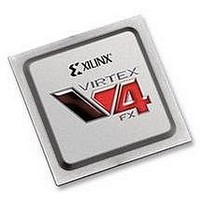
XC4VFX20-10FFG672C Xilinx Inc, XC4VFX20-10FFG672C Datasheet - Page 70

XC4VFX20-10FFG672C
Manufacturer Part Number
XC4VFX20-10FFG672C
Description
IC FPGA VIRTEX-4 FX 20K 672-FBGA
Manufacturer
Xilinx Inc
Series
Virtex™-4r
Datasheets
1.XC4VFX12-10FFG668C.pdf
(58 pages)
2.XC4VFX12-10FFG668C.pdf
(9 pages)
3.XC4VFX12-10FFG668C.pdf
(406 pages)
Specifications of XC4VFX20-10FFG672C
Total Ram Bits
1253376
Number Of Logic Elements/cells
19224
Number Of Labs/clbs
2136
Number Of I /o
320
Voltage - Supply
1.14 V ~ 1.26 V
Mounting Type
Surface Mount
Operating Temperature
0°C ~ 85°C
Package / Case
672-BBGA, FCBGA
No. Of Logic Blocks
19224
No. Of Macrocells
19224
No. Of Speed Grades
10
No. Of I/o's
320
Clock Management
DCM
I/o Supply Voltage
3.45V
Lead Free Status / RoHS Status
Lead free / RoHS Compliant
For Use With
HW-V4-ML405-UNI-G - EVALUATION PLATFORM VIRTEX-4
Number Of Gates
-
Lead Free Status / RoHS Status
Lead free / RoHS Compliant, Lead free / RoHS Compliant
Available stocks
Company
Part Number
Manufacturer
Quantity
Price
Company:
Part Number:
XC4VFX20-10FFG672C
Manufacturer:
ADVANTEK
Quantity:
314
Company:
Part Number:
XC4VFX20-10FFG672C
Manufacturer:
XilinxInc
Quantity:
3 000
Company:
Part Number:
XC4VFX20-10FFG672C
Manufacturer:
Xilinx Inc
Quantity:
10 000
Part Number:
XC4VFX20-10FFG672C
Manufacturer:
XILINX/赛灵思
Quantity:
20 000
- XC4VFX12-10FFG668C PDF datasheet
- XC4VFX12-10FFG668C PDF datasheet #2
- XC4VFX12-10FFG668C PDF datasheet #3
- Current page: 70 of 406
- Download datasheet (6Mb)
Chapter 2: Digital Clock Managers (DCMs)
DCM Design Guidelines
70
STARTUP_WAIT Attribute
Clock Deskew
Clock Deskew Operation
Refer to
relationship with the CLKOUT_PHASE_SHIFT and PHASE_SHIFT attributes.
The STARTUP_WAIT attribute determines whether the DCM waits in one of the startup
cycles for the DCM to lock. The possible values for this attribute are TRUE and FALSE. The
default value is FALSE. When STARTUP_WAIT is set to TRUE, and the LCK_cycle BitGen
option is used, then the configuration startup sequence waits in the startup cycle specified
by LCK_cycle until the DCM is locked.
This section provides a detailed guidelines on using the Virtex-4 FPGA DCM.
The Virtex-4 FPGA DCM offers a fully digital, dedicated, on-chip clock deskew. The
deskew feature provides zero propagation delay between the source clock and output
clock, low clock skew among output clock signals distributed throughout the device, and
advanced clock domain control.
The deskew feature also functions as a clock mirror of a board-level clock serving multiple
devices. This is achieved by driving the CLK0 output off-chip to the board (and to other
devices on the board) and then bringing the clock back in as a feedback clock. See the
“Application Examples”
simplifies and improves system-level design involving high-fanout, high-performance
clocks.
The deskew feature utilizes the DLL circuit in the DCM. In its simplest form, the DLL
consists of a single variable delay line (containing individual small delay elements or
buffers) and control logic. The incoming clock drives the delay line. The output of every
delay element represents a version of the incoming clock (CLKIN) delayed at a different
point. The clock distribution network routes the clock to all internal registers and to the
clock feedback CLKFB pin. The control logic contains a phase detector and a delay-line
selector. The phase detector compares the incoming clock signal (CLKIN) against a
feedback input (CLKFB) and steers the delay-line selector, essentially adding delay to the
DCM output until the CLKIN and CLKFB coincide, putting the two clocks 360° out-of-
phase, (thus, in phase). When the edges from the input clock line up with the edges from
the feedback clock, the DCM achieves a lock. The two clocks have no discernible
difference. Thus, the DCM output clock compensates for the delay in the clock distribution
network, effectively removing the delay between the source clock and its loads. The size of
each intrinsic delay element is a DCM_TAP (see the AC Characteristics table in the
Data
Sheet).
“Phase Shifting,” page 76
Figure 2-3
illustrates a simplified DLL circuit.
section. Taking advantage of the deskew feature greatly
www.xilinx.com
for information on the phase-shifting operation and its
UG070 (v2.6) December 1, 2008
Virtex-4 FPGA User Guide
Virtex-4
R
Related parts for XC4VFX20-10FFG672C
Image
Part Number
Description
Manufacturer
Datasheet
Request
R

Part Number:
Description:
IC FPGA VIRTEX-4 FX 20K 672-FBGA
Manufacturer:
Xilinx Inc
Datasheet:

Part Number:
Description:
IC FPGA VIRTEX-4 FX 20K 672-FBGA
Manufacturer:
Xilinx Inc
Datasheet:

Part Number:
Description:
IC FPGA VIRTEX-4FX 672FFBGA
Manufacturer:
Xilinx Inc
Datasheet:

Part Number:
Description:
IC FPGA VIRTEX-4 FX 20K 672-FBGA
Manufacturer:
Xilinx Inc
Datasheet:

Part Number:
Description:
IC FPGA VIRTEX-4FX 672FFBGA
Manufacturer:
Xilinx Inc
Datasheet:

Part Number:
Description:
DC and Switching Characteristics
Manufacturer:
XILINX [Xilinx, Inc]
Datasheet:

Part Number:
Description:
IC CPLD .8K 36MCELL 44-VQFP
Manufacturer:
Xilinx Inc
Datasheet:

Part Number:
Description:
IC CPLD 72MCRCELL 10NS 44VQFP
Manufacturer:
Xilinx Inc
Datasheet:

Part Number:
Description:
IC CPLD 1.6K 72MCELL 64-VQFP
Manufacturer:
Xilinx Inc
Datasheet:

Part Number:
Description:
IC CR-II CPLD 64MCELL 44-VQFP
Manufacturer:
Xilinx Inc
Datasheet:

Part Number:
Description:
IC CPLD 1.6K 72MCELL 100-TQFP
Manufacturer:
Xilinx Inc
Datasheet:

Part Number:
Description:
IC CR-II CPLD 64MCELL 56-BGA
Manufacturer:
Xilinx Inc
Datasheet:

Part Number:
Description:
IC CPLD 72MCRCELL 7.5NS 44VQFP
Manufacturer:
Xilinx Inc
Datasheet:

Part Number:
Description:
IC CR-II CPLD 64MCELL 100-VQFP
Manufacturer:
Xilinx Inc
Datasheet:

Part Number:
Description:
IC CPLD 1.6K 72MCELL 100-TQFP
Manufacturer:
Xilinx Inc
Datasheet:


