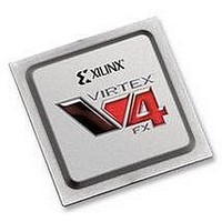
XC4VFX20-10FFG672C Xilinx Inc, XC4VFX20-10FFG672C Datasheet - Page 55

XC4VFX20-10FFG672C
Manufacturer Part Number
XC4VFX20-10FFG672C
Description
IC FPGA VIRTEX-4 FX 20K 672-FBGA
Manufacturer
Xilinx Inc
Series
Virtex™-4r
Datasheets
1.XC4VFX12-10FFG668C.pdf
(58 pages)
2.XC4VFX12-10FFG668C.pdf
(9 pages)
3.XC4VFX12-10FFG668C.pdf
(406 pages)
Specifications of XC4VFX20-10FFG672C
Total Ram Bits
1253376
Number Of Logic Elements/cells
19224
Number Of Labs/clbs
2136
Number Of I /o
320
Voltage - Supply
1.14 V ~ 1.26 V
Mounting Type
Surface Mount
Operating Temperature
0°C ~ 85°C
Package / Case
672-BBGA, FCBGA
No. Of Logic Blocks
19224
No. Of Macrocells
19224
No. Of Speed Grades
10
No. Of I/o's
320
Clock Management
DCM
I/o Supply Voltage
3.45V
Lead Free Status / RoHS Status
Lead free / RoHS Compliant
For Use With
HW-V4-ML405-UNI-G - EVALUATION PLATFORM VIRTEX-4
Number Of Gates
-
Lead Free Status / RoHS Status
Lead free / RoHS Compliant, Lead free / RoHS Compliant
Available stocks
Company
Part Number
Manufacturer
Quantity
Price
Company:
Part Number:
XC4VFX20-10FFG672C
Manufacturer:
ADVANTEK
Quantity:
314
Company:
Part Number:
XC4VFX20-10FFG672C
Manufacturer:
XilinxInc
Quantity:
3 000
Company:
Part Number:
XC4VFX20-10FFG672C
Manufacturer:
Xilinx Inc
Quantity:
10 000
Part Number:
XC4VFX20-10FFG672C
Manufacturer:
XILINX/赛灵思
Quantity:
20 000
- XC4VFX12-10FFG668C PDF datasheet
- XC4VFX12-10FFG668C PDF datasheet #2
- XC4VFX12-10FFG668C PDF datasheet #3
- Current page: 55 of 406
- Download datasheet (6Mb)
Digital Clock Managers (DCMs)
DCM Summary
Virtex-4 FPGA User Guide
UG070 (v2.6) December 1, 2008
R
The Virtex®-4 FPGA Digital Clock Managers (DCMs) provide a wide range of powerful
clock management features:
•
•
•
Clock Deskew
The DCM contains a delay-locked loop (DLL) to completely eliminate clock
distribution delays, by deskewing the DCM's output clocks with respect to the input
clock. The DLL contains delay elements (individual small buffers) and control logic.
The incoming clock drives a chain of delay elements, thus the output of every delay
element represents a version of the incoming clock delayed at a different point.
The control logic contains a phase detector and a delay-line selector. The phase
detector compares the incoming clock signal (CLKIN) against a feedback input
(CLKFB) and steers the delay line selector, essentially adding delay to the output of
DCM until the CLKIN and CLKFB coincide.
Frequency Synthesis
Separate outputs provide a doubled frequency (CLK2X and CLK2X180). Another
output, CLKDV, provides a frequency that is a specified fraction of the input
frequency.
Two other outputs, CLKFX and CLKFX180, provide an output frequency derived from
the input clock by simultaneous frequency division and multiplication. The user can
specify any integer multiplier (M) and divisor (D) within the range specified in the
DCM Timing Parameters section of the
determines the appropriate tap selection, to make the output edge coincide with the
input clock whenever mathematically possible. For example, M = 9 and D = 5,
multiply the frequency by 1.8, and the output rising edge is coincident with the input
rising edge after every fifth input period, or after every ninth output period.
Phase Shifting
The DCM allows coarse and fine-grained phase shifting. The coarse phase shifting
uses the 90°, 180°, and 270° phases of CLK0 to make CLK90, CLK180, and CLK270
clock outputs. The 180° phase of CLK2X and CLKFX provide the respective CLK2X180
and CLKFX180 clock outputs.
There are also four modes of fine-grained phase-shifting; fixed, variable-positive,
variable-center, and direct modes. Fine-grained phase shifting allows all DCM output
clocks to be phase-shifted with respect to CLKIN while maintaining the relationship
between the coarse phase outputs. With fixed mode, a fixed fraction of phase shift can
be defined during configuration and in multiples of the clock period divided by 256.
Using the variable-positive and variable-center modes the phase can be dynamically
and repetitively moved forward and backwards by 1/256 of the clock period. With the
www.xilinx.com
Virtex-4 Data
Sheet. An internal calculator
Chapter 2
55
Related parts for XC4VFX20-10FFG672C
Image
Part Number
Description
Manufacturer
Datasheet
Request
R

Part Number:
Description:
IC FPGA VIRTEX-4 FX 20K 672-FBGA
Manufacturer:
Xilinx Inc
Datasheet:

Part Number:
Description:
IC FPGA VIRTEX-4 FX 20K 672-FBGA
Manufacturer:
Xilinx Inc
Datasheet:

Part Number:
Description:
IC FPGA VIRTEX-4FX 672FFBGA
Manufacturer:
Xilinx Inc
Datasheet:

Part Number:
Description:
IC FPGA VIRTEX-4 FX 20K 672-FBGA
Manufacturer:
Xilinx Inc
Datasheet:

Part Number:
Description:
IC FPGA VIRTEX-4FX 672FFBGA
Manufacturer:
Xilinx Inc
Datasheet:

Part Number:
Description:
DC and Switching Characteristics
Manufacturer:
XILINX [Xilinx, Inc]
Datasheet:

Part Number:
Description:
IC CPLD .8K 36MCELL 44-VQFP
Manufacturer:
Xilinx Inc
Datasheet:

Part Number:
Description:
IC CPLD 72MCRCELL 10NS 44VQFP
Manufacturer:
Xilinx Inc
Datasheet:

Part Number:
Description:
IC CPLD 1.6K 72MCELL 64-VQFP
Manufacturer:
Xilinx Inc
Datasheet:

Part Number:
Description:
IC CR-II CPLD 64MCELL 44-VQFP
Manufacturer:
Xilinx Inc
Datasheet:

Part Number:
Description:
IC CPLD 1.6K 72MCELL 100-TQFP
Manufacturer:
Xilinx Inc
Datasheet:

Part Number:
Description:
IC CR-II CPLD 64MCELL 56-BGA
Manufacturer:
Xilinx Inc
Datasheet:

Part Number:
Description:
IC CPLD 72MCRCELL 7.5NS 44VQFP
Manufacturer:
Xilinx Inc
Datasheet:

Part Number:
Description:
IC CR-II CPLD 64MCELL 100-VQFP
Manufacturer:
Xilinx Inc
Datasheet:

Part Number:
Description:
IC CPLD 1.6K 72MCELL 100-TQFP
Manufacturer:
Xilinx Inc
Datasheet:


