D12363VTE33 Renesas Electronics America, D12363VTE33 Datasheet - Page 195
D12363VTE33
Manufacturer Part Number
D12363VTE33
Description
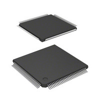
MCU 3V 0K 120-TQFP
Manufacturer
Renesas Electronics America
Series
H8® H8S/2300r
Datasheet
1.DF2368VTE34V.pdf
(1044 pages)
Specifications of D12363VTE33
Core Processor
H8S/2000
Core Size
16-Bit
Speed
33MHz
Connectivity
I²C, IrDA, SCI, SmartCard
Peripherals
DMA, POR, PWM, WDT
Number Of I /o
84
Program Memory Type
ROMless
Ram Size
16K x 8
Voltage - Supply (vcc/vdd)
3 V ~ 3.6 V
Data Converters
A/D 10x10b, D/A 2x8b
Oscillator Type
Internal
Operating Temperature
-20°C ~ 75°C
Package / Case
120-TQFP, 120-VQFP
Lead Free Status / RoHS Status
Contains lead / RoHS non-compliant
Eeprom Size
-
Program Memory Size
-
Other names
HD6412363VTE33
HD6412363VTE33
HD6412363VTE33
Available stocks
Company
Part Number
Manufacturer
Quantity
Price
Company:

Part Number:
D12363VTE33V
Manufacturer:
Renesas Electronics America
Quantity:
10 000


6.3.8
DRAMCR is used to make DRAM/synchronous DRAM interface settings.
Bit
15
14
13
12
11
Bit Name
OEE
RAST
−
CAST
−
DRAM Control Register (DRAMCR)
Initial Value
0
0
0
0
0
R/W
R/W
R/W
R/W
R/W
R/W
Description
OE Output Enable
The OE signal used when EDO page mode
DRAM is connected can be output from the
(OE) pin. The OE signal is common to all
areas designated as DRAM space.
0: OE signal output disabled
1: OE signal output enabled
RAS Assertion Timing Select
Selects whether, in DRAM access, the RAS
signal is asserted from the start of the T
(rising edge of φ) or from the falling edge of φ.
Figure 6.4 shows the relationship between the
RAST bit setting and the RAS assertion timing.
The setting of this bit applies to all areas
designated as DRAM space.
0: RAS is asserted from φ falling edge in T
1: RAS is asserted from start of T
Reserved
Though this bit can be read from or written to,
the write value should always be 0.
Column Address Output Cycle Number Select
Selects whether the column address output
cycle in DRAM access comprises 3 states or 2
states. The setting of this bit applies to all
areas designated as DRAM space.
0: 2-state column address output cycle
1: 3-state column address output cycle
Reserved
Though this bit can be read from or written to,
the write value should always be 0.
(OE) pin can be used as I/O port
cycle
Rev.6.00 Mar. 18, 2009 Page 135 of 980
Section 6 Bus Controller (BSC)
REJ09B0050-0600
r
cycle
r
cycle
r
Related parts for D12363VTE33
Image
Part Number
Description
Manufacturer
Datasheet
Request
R

Part Number:
Description:
KIT STARTER FOR M16C/29
Manufacturer:
Renesas Electronics America
Datasheet:

Part Number:
Description:
KIT STARTER FOR R8C/2D
Manufacturer:
Renesas Electronics America
Datasheet:

Part Number:
Description:
R0K33062P STARTER KIT
Manufacturer:
Renesas Electronics America
Datasheet:

Part Number:
Description:
KIT STARTER FOR R8C/23 E8A
Manufacturer:
Renesas Electronics America
Datasheet:

Part Number:
Description:
KIT STARTER FOR R8C/25
Manufacturer:
Renesas Electronics America
Datasheet:

Part Number:
Description:
KIT STARTER H8S2456 SHARPE DSPLY
Manufacturer:
Renesas Electronics America
Datasheet:

Part Number:
Description:
KIT STARTER FOR R8C38C
Manufacturer:
Renesas Electronics America
Datasheet:

Part Number:
Description:
KIT STARTER FOR R8C35C
Manufacturer:
Renesas Electronics America
Datasheet:

Part Number:
Description:
KIT STARTER FOR R8CL3AC+LCD APPS
Manufacturer:
Renesas Electronics America
Datasheet:
Part Number:
Description:
KIT STARTER FOR RX610
Manufacturer:
Renesas Electronics America
Datasheet:

Part Number:
Description:
KIT STARTER FOR R32C/118
Manufacturer:
Renesas Electronics America
Datasheet:

Part Number:
Description:
KIT DEV RSK-R8C/26-29
Manufacturer:
Renesas Electronics America
Datasheet:

Part Number:
Description:
KIT STARTER FOR SH7124
Manufacturer:
Renesas Electronics America
Datasheet:

Part Number:
Description:
KIT STARTER FOR H8SX/1622
Manufacturer:
Renesas Electronics America
Datasheet:

Part Number:
Description:
KIT DEV FOR SH7203
Manufacturer:
Renesas Electronics America
Datasheet: