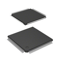
D12363VTE33 Renesas Electronics America, D12363VTE33 Datasheet - Page 771

D12363VTE33
Manufacturer Part Number
D12363VTE33
Description
MCU 3V 0K 120-TQFP
Manufacturer
Renesas Electronics America
Series
H8® H8S/2300r
Datasheet
1.DF2368VTE34V.pdf
(1044 pages)
Specifications of D12363VTE33
Core Processor
H8S/2000
Core Size
16-Bit
Speed
33MHz
Connectivity
I²C, IrDA, SCI, SmartCard
Peripherals
DMA, POR, PWM, WDT
Number Of I /o
84
Program Memory Type
ROMless
Ram Size
16K x 8
Voltage - Supply (vcc/vdd)
3 V ~ 3.6 V
Data Converters
A/D 10x10b, D/A 2x8b
Oscillator Type
Internal
Operating Temperature
-20°C ~ 75°C
Package / Case
120-TQFP, 120-VQFP
Lead Free Status / RoHS Status
Contains lead / RoHS non-compliant
Eeprom Size
-
Program Memory Size
-
Other names
HD6412363VTE33
HD6412363VTE33
HD6412363VTE33
Available stocks
Company
Part Number
Manufacturer
Quantity
Price
Company:
Part Number:
D12363VTE33V
Manufacturer:
Renesas Electronics America
Quantity:
10 000
- Current page: 771 of 1044
- Download datasheet (6Mb)
The FLMCR1, FLMCR2, EBR1, and EBR2 settings are retained, but program mode or erase
mode is forcibly aborted at the point at which the error occurred. Program mode or erase mode
cannot be re-entered by re-setting the P or E bit. However, since PV and EV bit setting is enabled,
and a transition can be made to verify mode. The error protection state can be canceled by a reset
or in hardware standby mode.
19.9
In programmer mode, a PROM programmer can perform programming/erasing via a socket
adapter, just like for a discrete flash memory. Use a PROM programmer which supports the
Renesas 512-kbyte flash memory on-chip MCU device type (FZTAT512V3A). A 12-MHz input
clock is needed.
19.10
In user mode, the flash memory will operate in either of the following states:
• Normal operating mode
• Standby mode
Table 19.7 shows the correspondence between the operating modes of this LSI and the flash
memory. When the flash memory returns to normal operation from a standby state, a power
supply circuit stabilization period is needed. When the flash memory returns to its normal
operating state, bits STS3 to STS0 in SBYCR must be set to provide a wait time of at least 100 µs,
even when the external clock is being used.
Table 19.7 Flash Memory Operating States
Operating Mode
Active mode
Sleep mode
Standby mode
The flash memory can be read.
All flash memory circuits are halted.
Programmer Mode
Power-Down States for Flash Memory
Section 19 Flash Memory (0.35-μm F-ZTAT Version)
Flash Memory Operating State
Normal operating state
Normal operating state
Standby state
Rev.6.00 Mar. 18, 2009 Page 711 of 980
REJ09B0050-0600
Related parts for D12363VTE33
Image
Part Number
Description
Manufacturer
Datasheet
Request
R

Part Number:
Description:
KIT STARTER FOR M16C/29
Manufacturer:
Renesas Electronics America
Datasheet:

Part Number:
Description:
KIT STARTER FOR R8C/2D
Manufacturer:
Renesas Electronics America
Datasheet:

Part Number:
Description:
R0K33062P STARTER KIT
Manufacturer:
Renesas Electronics America
Datasheet:

Part Number:
Description:
KIT STARTER FOR R8C/23 E8A
Manufacturer:
Renesas Electronics America
Datasheet:

Part Number:
Description:
KIT STARTER FOR R8C/25
Manufacturer:
Renesas Electronics America
Datasheet:

Part Number:
Description:
KIT STARTER H8S2456 SHARPE DSPLY
Manufacturer:
Renesas Electronics America
Datasheet:

Part Number:
Description:
KIT STARTER FOR R8C38C
Manufacturer:
Renesas Electronics America
Datasheet:

Part Number:
Description:
KIT STARTER FOR R8C35C
Manufacturer:
Renesas Electronics America
Datasheet:

Part Number:
Description:
KIT STARTER FOR R8CL3AC+LCD APPS
Manufacturer:
Renesas Electronics America
Datasheet:

Part Number:
Description:
KIT STARTER FOR RX610
Manufacturer:
Renesas Electronics America
Datasheet:

Part Number:
Description:
KIT STARTER FOR R32C/118
Manufacturer:
Renesas Electronics America
Datasheet:

Part Number:
Description:
KIT DEV RSK-R8C/26-29
Manufacturer:
Renesas Electronics America
Datasheet:

Part Number:
Description:
KIT STARTER FOR SH7124
Manufacturer:
Renesas Electronics America
Datasheet:

Part Number:
Description:
KIT STARTER FOR H8SX/1622
Manufacturer:
Renesas Electronics America
Datasheet:

Part Number:
Description:
KIT DEV FOR SH7203
Manufacturer:
Renesas Electronics America
Datasheet:


