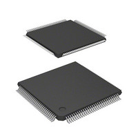
D12363VTE33 Renesas Electronics America, D12363VTE33 Datasheet - Page 47

D12363VTE33
Manufacturer Part Number
D12363VTE33
Description
MCU 3V 0K 120-TQFP
Manufacturer
Renesas Electronics America
Series
H8® H8S/2300r
Datasheet
1.DF2368VTE34V.pdf
(1044 pages)
Specifications of D12363VTE33
Core Processor
H8S/2000
Core Size
16-Bit
Speed
33MHz
Connectivity
I²C, IrDA, SCI, SmartCard
Peripherals
DMA, POR, PWM, WDT
Number Of I /o
84
Program Memory Type
ROMless
Ram Size
16K x 8
Voltage - Supply (vcc/vdd)
3 V ~ 3.6 V
Data Converters
A/D 10x10b, D/A 2x8b
Oscillator Type
Internal
Operating Temperature
-20°C ~ 75°C
Package / Case
120-TQFP, 120-VQFP
Lead Free Status / RoHS Status
Contains lead / RoHS non-compliant
Eeprom Size
-
Program Memory Size
-
Other names
HD6412363VTE33
HD6412363VTE33
HD6412363VTE33
Available stocks
Company
Part Number
Manufacturer
Quantity
Price
Company:
Part Number:
D12363VTE33V
Manufacturer:
Renesas Electronics America
Quantity:
10 000
- Current page: 47 of 1044
- Download datasheet (6Mb)
Figure 10.50 Contention between TGR Write and Input Capture ............................................... 482
Figure 10.51 Contention between Buffer Register Write and Input Capture............................... 483
Figure 10.52 Contention between Overflow and Counter Clearing ............................................ 483
Figure 10.53 Contention between TCNT Write and Overflow.................................................... 484
Section 11 Programmable Pulse Generator (PPG)
Figure 11.1 Block Diagram of PPG........................................................................................... 486
Figure 11.2 Overview Diagram of PPG..................................................................................... 495
Figure 11.3 Timing of Transfer and Output of NDR Contents (Example) ................................ 496
Figure 11.4 Setup Procedure for Normal Pulse Output (Example)............................................ 497
Figure 11.5 Normal Pulse Output Example (Five-Phase Pulse Output) .................................... 498
Figure 11.6 Non-Overlapping Pulse Output .............................................................................. 499
Figure 11.7 Non-Overlapping Operation and NDR Write Timing ............................................ 500
Figure 11.8 Setup Procedure for Non-Overlapping Pulse Output (Example)............................ 501
Figure 11.9 Non-Overlapping Pulse Output Example (Four-Phase Complementary)............... 502
Figure 11.10 Inverted Pulse Output (Example) ........................................................................... 504
Figure 11.11 Pulse Output Triggered by Input Capture (Example)............................................. 505
Section 12 8-Bit Timers (TMR)
Figure 12.1 Block Diagram of 8-Bit Timer Module.................................................................. 508
Figure 12.2 Example of Pulse Output........................................................................................ 516
Figure 12.3 Count Timing for Internal Clock Input................................................................... 516
Figure 12.4 Count Timing for External Clock Input ................................................................. 517
Figure 12.5 Timing of CMF Setting .......................................................................................... 517
Figure 12.6 Timing of Timer Output ......................................................................................... 518
Figure 12.7 Timing of Compare Match Clear ........................................................................... 518
Figure 12.8 Timing of Clearance by External Reset.................................................................. 519
Figure 12.9 Timing of OVF Setting........................................................................................... 519
Figure 12.10 Contention between TCNT Write and Clear .......................................................... 522
Figure 12.11 Contention between TCNT Write and Increment................................................... 523
Figure 12.12 Contention between TCOR Write and Compare Match......................................... 524
Section 13 Watchdog Timer
Figure 13.1 Block Diagram of WDT ......................................................................................... 530
Figure 13.2 Operation in Watchdog Timer Mode...................................................................... 535
Figure 13.3 Operation in Interval Timer Mode ......................................................................... 536
Figure 13.4 Writing to TCNT, TCSR, and RSTCSR................................................................. 537
Figure 13.5 Contention between TCNT Write and Increment................................................... 538
Figure 13.6 Circuit for System Reset by WDTOVF Signal (Example)..................................... 539
Rev.6.00 Mar. 18, 2009 Page xlv of lviii
REJ09B0050-0600
Related parts for D12363VTE33
Image
Part Number
Description
Manufacturer
Datasheet
Request
R

Part Number:
Description:
KIT STARTER FOR M16C/29
Manufacturer:
Renesas Electronics America
Datasheet:

Part Number:
Description:
KIT STARTER FOR R8C/2D
Manufacturer:
Renesas Electronics America
Datasheet:

Part Number:
Description:
R0K33062P STARTER KIT
Manufacturer:
Renesas Electronics America
Datasheet:

Part Number:
Description:
KIT STARTER FOR R8C/23 E8A
Manufacturer:
Renesas Electronics America
Datasheet:

Part Number:
Description:
KIT STARTER FOR R8C/25
Manufacturer:
Renesas Electronics America
Datasheet:

Part Number:
Description:
KIT STARTER H8S2456 SHARPE DSPLY
Manufacturer:
Renesas Electronics America
Datasheet:

Part Number:
Description:
KIT STARTER FOR R8C38C
Manufacturer:
Renesas Electronics America
Datasheet:

Part Number:
Description:
KIT STARTER FOR R8C35C
Manufacturer:
Renesas Electronics America
Datasheet:

Part Number:
Description:
KIT STARTER FOR R8CL3AC+LCD APPS
Manufacturer:
Renesas Electronics America
Datasheet:

Part Number:
Description:
KIT STARTER FOR RX610
Manufacturer:
Renesas Electronics America
Datasheet:

Part Number:
Description:
KIT STARTER FOR R32C/118
Manufacturer:
Renesas Electronics America
Datasheet:

Part Number:
Description:
KIT DEV RSK-R8C/26-29
Manufacturer:
Renesas Electronics America
Datasheet:

Part Number:
Description:
KIT STARTER FOR SH7124
Manufacturer:
Renesas Electronics America
Datasheet:

Part Number:
Description:
KIT STARTER FOR H8SX/1622
Manufacturer:
Renesas Electronics America
Datasheet:

Part Number:
Description:
KIT DEV FOR SH7203
Manufacturer:
Renesas Electronics America
Datasheet:


