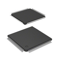
D12363VTE33 Renesas Electronics America, D12363VTE33 Datasheet - Page 719

D12363VTE33
Manufacturer Part Number
D12363VTE33
Description
MCU 3V 0K 120-TQFP
Manufacturer
Renesas Electronics America
Series
H8® H8S/2300r
Datasheet
1.DF2368VTE34V.pdf
(1044 pages)
Specifications of D12363VTE33
Core Processor
H8S/2000
Core Size
16-Bit
Speed
33MHz
Connectivity
I²C, IrDA, SCI, SmartCard
Peripherals
DMA, POR, PWM, WDT
Number Of I /o
84
Program Memory Type
ROMless
Ram Size
16K x 8
Voltage - Supply (vcc/vdd)
3 V ~ 3.6 V
Data Converters
A/D 10x10b, D/A 2x8b
Oscillator Type
Internal
Operating Temperature
-20°C ~ 75°C
Package / Case
120-TQFP, 120-VQFP
Lead Free Status / RoHS Status
Contains lead / RoHS non-compliant
Eeprom Size
-
Program Memory Size
-
Other names
HD6412363VTE33
HD6412363VTE33
HD6412363VTE33
Available stocks
Company
Part Number
Manufacturer
Quantity
Price
Company:
Part Number:
D12363VTE33V
Manufacturer:
Renesas Electronics America
Quantity:
10 000
- Current page: 719 of 1044
- Download datasheet (6Mb)
Table 15.4 Time for monitoring SCL
CKS3
1
Note:
15.7
1. Issue (retransmit) the start/stop conditions after the fall of the ninth clock is confirmed.
2. Control WAIT in the I
0
Check SCLO in the I
When the start/stop conditions are issued (retransmitted) at the specific timing under the
following condition (i) or (ii), such conditions may not be output successfully. This does not
occur in other cases.
(i) When the rising of SCL falls behind the time specified in section 15.6, Bit Synchronous
(ii) When the bit synchronous circuit is activated by extending the low period of eighth and
When WAIT is set to 1, and SCL is driven low for two or more transfer clocks by the slave
device at the eighth and ninth clocks, the high period of ninth clock may be shortened. This
does not occur in other cases.
Circuit, by the load of the SCL bus (load capacitance or pull-up resistance)
ninth clocks, that is driven by the slave device
*
Usage Notes
If the operating frequency exceeds 20 MHz, it may not be possible to maintain the
prescribed transfer rate under certain load conditions. A setting other than 7.5 tcyc
should therefore be used.
SCL monitor
timing reference
clock
Internal SCL
CKS2
0
1
0
1
SCL
Figure 15.18 Timing of the Bit Synchronous Circuit
2
C control register B (ICCRB)* to confirm the fall of the ninth clock.
2
C bus mode register (ICMR) to be set to 0.
17.5 tcyc
41.5 tcyc
Time for monitoring SCL
7.5 tcyc *
19.5 tcyc
VIH
Section 15 I
Rev.6.00 Mar. 18, 2009 Page 659 of 980
2
C Bus Interface2 (IIC2) (Option)
REJ09B0050-0600
Related parts for D12363VTE33
Image
Part Number
Description
Manufacturer
Datasheet
Request
R

Part Number:
Description:
KIT STARTER FOR M16C/29
Manufacturer:
Renesas Electronics America
Datasheet:

Part Number:
Description:
KIT STARTER FOR R8C/2D
Manufacturer:
Renesas Electronics America
Datasheet:

Part Number:
Description:
R0K33062P STARTER KIT
Manufacturer:
Renesas Electronics America
Datasheet:

Part Number:
Description:
KIT STARTER FOR R8C/23 E8A
Manufacturer:
Renesas Electronics America
Datasheet:

Part Number:
Description:
KIT STARTER FOR R8C/25
Manufacturer:
Renesas Electronics America
Datasheet:

Part Number:
Description:
KIT STARTER H8S2456 SHARPE DSPLY
Manufacturer:
Renesas Electronics America
Datasheet:

Part Number:
Description:
KIT STARTER FOR R8C38C
Manufacturer:
Renesas Electronics America
Datasheet:

Part Number:
Description:
KIT STARTER FOR R8C35C
Manufacturer:
Renesas Electronics America
Datasheet:

Part Number:
Description:
KIT STARTER FOR R8CL3AC+LCD APPS
Manufacturer:
Renesas Electronics America
Datasheet:

Part Number:
Description:
KIT STARTER FOR RX610
Manufacturer:
Renesas Electronics America
Datasheet:

Part Number:
Description:
KIT STARTER FOR R32C/118
Manufacturer:
Renesas Electronics America
Datasheet:

Part Number:
Description:
KIT DEV RSK-R8C/26-29
Manufacturer:
Renesas Electronics America
Datasheet:

Part Number:
Description:
KIT STARTER FOR SH7124
Manufacturer:
Renesas Electronics America
Datasheet:

Part Number:
Description:
KIT STARTER FOR H8SX/1622
Manufacturer:
Renesas Electronics America
Datasheet:

Part Number:
Description:
KIT DEV FOR SH7203
Manufacturer:
Renesas Electronics America
Datasheet:


