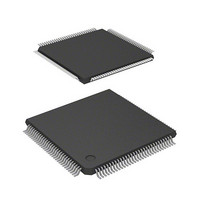
D12363VTE33 Renesas Electronics America, D12363VTE33 Datasheet - Page 75

D12363VTE33
Manufacturer Part Number
D12363VTE33
Description
MCU 3V 0K 120-TQFP
Manufacturer
Renesas Electronics America
Series
H8® H8S/2300r
Datasheet
1.DF2368VTE34V.pdf
(1044 pages)
Specifications of D12363VTE33
Core Processor
H8S/2000
Core Size
16-Bit
Speed
33MHz
Connectivity
I²C, IrDA, SCI, SmartCard
Peripherals
DMA, POR, PWM, WDT
Number Of I /o
84
Program Memory Type
ROMless
Ram Size
16K x 8
Voltage - Supply (vcc/vdd)
3 V ~ 3.6 V
Data Converters
A/D 10x10b, D/A 2x8b
Oscillator Type
Internal
Operating Temperature
-20°C ~ 75°C
Package / Case
120-TQFP, 120-VQFP
Lead Free Status / RoHS Status
Contains lead / RoHS non-compliant
Eeprom Size
-
Program Memory Size
-
Other names
HD6412363VTE33
HD6412363VTE33
HD6412363VTE33
Available stocks
Company
Part Number
Manufacturer
Quantity
Price
Company:
Part Number:
D12363VTE33V
Manufacturer:
Renesas Electronics America
Quantity:
10 000
- Current page: 75 of 1044
- Download datasheet (6Mb)
Type
System control RES
Address bus
Data bus
Bus control
STBY
EMLE
A23 to
A0
D15 to
D0
CS7 to
CS0
AS
RD
HWR
LWR
BREQ
BREQO
Symbol
Pin No.
TFP-120
77
88
30
29 to 23,
21 to 18,
16 to 9,
7 to 3
68 to 61,
59,
57 to 51
29,71,70,
106,
92 to 89
75
74
73
72
108
106
85
96
34
33 to 27,
25 to 22,
20 to 13,
11 to 7
76 to 69,
65,
63 to 57
33,79,78,
116,102,
101,98,97
83
82
81
80
118
116
QFP-128 *
1
Input
Input
Input
Output Address output pins.
Input/
output
Output Signals that select division areas 7
Output When this pin is low, it indicates
Output When this pin is low, it indicates
Output Strobe signal indicating that
Output Strobe signal indicating that
Input
Input
I/O
Rev.6.00 Mar. 18, 2009 Page 15 of 980
Reset pin. When this pin is driven
low, the chip is reset.
When this pin is driven low, a
transition is made to hardware
standby mode.
Enables emulator. This pin should
be connected to the power supply
(0 V).
These pins constitute a bidirectional
data bus.
to 0 in the external address space.
that address output on the address
bus is valid.
that the external address space is
being read.
external address space is to be
written, and the upper half (D15 to
D8) of the data bus is enabled.
Write enable signal for accessing
the DRAM space.
external address space is to be
written, and the lower half (D7 to
D0) of the data bus is enabled.
The external bus master requests
the bus to this LSI.
External bus request signal when
the internal bus master accesses
the external space in external bus
release state.
Function
Section 1 Overview
REJ09B0050-0600
Related parts for D12363VTE33
Image
Part Number
Description
Manufacturer
Datasheet
Request
R

Part Number:
Description:
KIT STARTER FOR M16C/29
Manufacturer:
Renesas Electronics America
Datasheet:

Part Number:
Description:
KIT STARTER FOR R8C/2D
Manufacturer:
Renesas Electronics America
Datasheet:

Part Number:
Description:
R0K33062P STARTER KIT
Manufacturer:
Renesas Electronics America
Datasheet:

Part Number:
Description:
KIT STARTER FOR R8C/23 E8A
Manufacturer:
Renesas Electronics America
Datasheet:

Part Number:
Description:
KIT STARTER FOR R8C/25
Manufacturer:
Renesas Electronics America
Datasheet:

Part Number:
Description:
KIT STARTER H8S2456 SHARPE DSPLY
Manufacturer:
Renesas Electronics America
Datasheet:

Part Number:
Description:
KIT STARTER FOR R8C38C
Manufacturer:
Renesas Electronics America
Datasheet:

Part Number:
Description:
KIT STARTER FOR R8C35C
Manufacturer:
Renesas Electronics America
Datasheet:

Part Number:
Description:
KIT STARTER FOR R8CL3AC+LCD APPS
Manufacturer:
Renesas Electronics America
Datasheet:

Part Number:
Description:
KIT STARTER FOR RX610
Manufacturer:
Renesas Electronics America
Datasheet:

Part Number:
Description:
KIT STARTER FOR R32C/118
Manufacturer:
Renesas Electronics America
Datasheet:

Part Number:
Description:
KIT DEV RSK-R8C/26-29
Manufacturer:
Renesas Electronics America
Datasheet:

Part Number:
Description:
KIT STARTER FOR SH7124
Manufacturer:
Renesas Electronics America
Datasheet:

Part Number:
Description:
KIT STARTER FOR H8SX/1622
Manufacturer:
Renesas Electronics America
Datasheet:

Part Number:
Description:
KIT DEV FOR SH7203
Manufacturer:
Renesas Electronics America
Datasheet:


