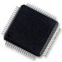
UPD78F0890GK(A)-GAJ-AX NEC, UPD78F0890GK(A)-GAJ-AX Datasheet - Page 36

UPD78F0890GK(A)-GAJ-AX
Manufacturer Part Number
UPD78F0890GK(A)-GAJ-AX
Description
8BIT MCU, 128K FLASH, 7K RAM, LQFP
Manufacturer
NEC
Datasheet
1.UPD78F0890GKA-GAJ-AX.pdf
(732 pages)
Specifications of UPD78F0890GK(A)-GAJ-AX
Controller Family/series
UPD78F
No. Of I/o's
55
Ram Memory Size
7KB
Cpu Speed
20MHz
No. Of Timers
10
No. Of Pwm
RoHS Compliant
Core Size
8bit
Program Memory Size
128KB
Oscillator Type
External, Internal
- Current page: 36 of 732
- Download datasheet (4Mb)
2.2.12 AV
2.2.13 AV
the same potential as the EV
2.2.14 RESET
2.2.15 REGC
pin to V
2.2.16 V
2.2.17 V
2.2.18 FLMD0
this pin to the flash programmer.
36
Connect to EV
This is the A/D converter reference voltage input pin.
When the A/D converter is not used, connect this pin directly to EV
This is the A/D converter ground potential pin. Even when the A/D converter is not used, always use this pin with
This is the active-low system reset input pin.
This is the pin for connecting regulator output (2.5 V) stabilization capacitance for internal operation. Connect this
V
EV
V
EV
This is a pin for setting flash memory programming mode.
Note Connect port 8 and port 9 directly to EV
DD
SS
Caution Keep the wiring length as short as possible for the broken-line part in the above figure.
DD
SS
is the ground potential pin for other than ports.
is the positive power supply pin for other than ports.
SS
is the ground potential pin for ports.
is the positive power supply pin for ports.
DD
SS
via a capacitor (0.47 to 1 µF: recommended).
REF
SS
and EV
and EV
SS
SS
DD
or V
SS
in the normal operation mode. In flash memory programming mode, be sure to connect
SS
pin or V
SS
pin.
CHAPTER 2 PIN FUNCTIONS
User’s Manual U17554EJ4V0UD
DD
when it is used as a digital port.
REGC
V
SS
DD
or V
DD
Note
.
Related parts for UPD78F0890GK(A)-GAJ-AX
Image
Part Number
Description
Manufacturer
Datasheet
Request
R

Part Number:
Description:
16/8 bit single-chip microcomputer
Manufacturer:
NEC
Datasheet:

Part Number:
Description:
Dual audio power amp circuit
Manufacturer:
NEC
Datasheet:

Part Number:
Description:
Dual comparator
Manufacturer:
NEC
Datasheet:

Part Number:
Description:
MOS type composite field effect transistor
Manufacturer:
NEC
Datasheet:

Part Number:
Description:
50 V/100 mA FET array incorporating 2 N-ch MOSFETs
Manufacturer:
NEC
Datasheet:

Part Number:
Description:
6-pin small MM high-frequency double transistor
Manufacturer:
NEC
Datasheet:

Part Number:
Description:
6-pin small MM high-frequency double transistor
Manufacturer:
NEC
Datasheet:

Part Number:
Description:
6-pin small MM high-frequency double transistor
Manufacturer:
NEC
Datasheet:

Part Number:
Description:
6-pin small MM high-frequency double transistor
Manufacturer:
NEC
Datasheet:

Part Number:
Description:
Twin transistors equipped with different model chips(6P small MM)
Manufacturer:
NEC
Datasheet:

Part Number:
Description:
Bipolar analog integrated circuit
Manufacturer:
NEC
Datasheet:


