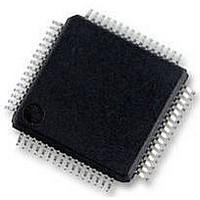
UPD78F0890GK(A)-GAJ-AX NEC, UPD78F0890GK(A)-GAJ-AX Datasheet - Page 82

UPD78F0890GK(A)-GAJ-AX
Manufacturer Part Number
UPD78F0890GK(A)-GAJ-AX
Description
8BIT MCU, 128K FLASH, 7K RAM, LQFP
Manufacturer
NEC
Datasheet
1.UPD78F0890GKA-GAJ-AX.pdf
(732 pages)
Specifications of UPD78F0890GK(A)-GAJ-AX
Controller Family/series
UPD78F
No. Of I/o's
55
Ram Memory Size
7KB
Cpu Speed
20MHz
No. Of Timers
10
No. Of Pwm
RoHS Compliant
Core Size
8bit
Program Memory Size
128KB
Oscillator Type
External, Internal
- Current page: 82 of 732
- Download datasheet (4Mb)
4.3 Memory Bank Select Register (BANK)
82
Notes 1. SM+ for 78K0/Fx2, ID78K0-QB
For details, see the RA78K0 Ver. 3.80 Assembler Package Operation User’s Manual (U17199E).
The memory bank select register (BANK) is used to select a memory bank to be used.
BANK can be set by an 8-bit memory manipulation instruction.
Reset signal generation clears BANK to 00H.
Caution Be sure to change the value of the BANK register in the common area (0000H to 7FFFH).
Memory Bank Number
Memory bank 0
Memory bank 1
Memory bank 2
Memory bank 3
Memory bank 4
Memory bank 5
Address: FFF3H After reset: 00H R/W
Symbol
2. Set the memory bank to be used by the memory bank select register (BANK) (see Figure 4-3).
BANK
If the value of the BANK register is changed in the bank area (8000H to BFFFH), an inadvertent
program loop occurs in the CPU. Therefore, never change the value of the BANK register in the
bank area.
CHAPTER 4 MEMORY BANK SELECT FUNCTION (
BANK2
7
0
0
0
0
0
1
1
08000H-0BFFFH
Figure 4-3. Format of Memory Bank Select Register (BANK)
Other than above
Table 4-1. Memory Bank Address Representation
BANK1
CPU Address
6
0
0
0
1
1
0
0
Note 2
BANK0
User’s Manual U17554EJ4V0UD
5
0
0
1
0
1
0
1
Common area (32 K) + memory bank 0 (16 K)
Common area (32 K) + memory bank 1 (16 K)
Common area (32 K) + memory bank 2 (16 K)
Common area (32 K) + memory bank 3 (16 K)
Setting prohibited
Setting prohibited
08000H-0BFFFH
0C000H-0FFFFH
10000H-13FFFH
14000H-17FFFH
18000H-1BFFFH
1C000H-1FFFFH
Flash Memory Real Address
4
0
μ
PD78F0889
3
0
PD78F0889, 78F0890 ONLY)
Bank setting
BANK2
2
Common area (32 K) +
memory bank 4 (16 K)
Common area (32 K) +
memory bank 5 (16 K)
08000H-0BFFFH
18000H-1BFFFH
28000H-2BFFFH
38000H-3BFFFH
48000H-4BFFFH
58000H-5BFFFH
Simulator and Debugger
Address Representation in
BANK1
μ
PD78F0890
1
BANK0
0
Note 1
Related parts for UPD78F0890GK(A)-GAJ-AX
Image
Part Number
Description
Manufacturer
Datasheet
Request
R

Part Number:
Description:
16/8 bit single-chip microcomputer
Manufacturer:
NEC
Datasheet:

Part Number:
Description:
Dual audio power amp circuit
Manufacturer:
NEC
Datasheet:

Part Number:
Description:
Dual comparator
Manufacturer:
NEC
Datasheet:

Part Number:
Description:
MOS type composite field effect transistor
Manufacturer:
NEC
Datasheet:

Part Number:
Description:
50 V/100 mA FET array incorporating 2 N-ch MOSFETs
Manufacturer:
NEC
Datasheet:

Part Number:
Description:
6-pin small MM high-frequency double transistor
Manufacturer:
NEC
Datasheet:

Part Number:
Description:
6-pin small MM high-frequency double transistor
Manufacturer:
NEC
Datasheet:

Part Number:
Description:
6-pin small MM high-frequency double transistor
Manufacturer:
NEC
Datasheet:

Part Number:
Description:
6-pin small MM high-frequency double transistor
Manufacturer:
NEC
Datasheet:

Part Number:
Description:
Twin transistors equipped with different model chips(6P small MM)
Manufacturer:
NEC
Datasheet:

Part Number:
Description:
Bipolar analog integrated circuit
Manufacturer:
NEC
Datasheet:


