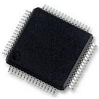
UPD78F0890GK(A)-GAJ-AX NEC, UPD78F0890GK(A)-GAJ-AX Datasheet - Page 614

UPD78F0890GK(A)-GAJ-AX
Manufacturer Part Number
UPD78F0890GK(A)-GAJ-AX
Description
8BIT MCU, 128K FLASH, 7K RAM, LQFP
Manufacturer
NEC
Datasheet
1.UPD78F0890GKA-GAJ-AX.pdf
(732 pages)
Specifications of UPD78F0890GK(A)-GAJ-AX
Controller Family/series
UPD78F
No. Of I/o's
55
Ram Memory Size
7KB
Cpu Speed
20MHz
No. Of Timers
10
No. Of Pwm
RoHS Compliant
Core Size
8bit
Program Memory Size
128KB
Oscillator Type
External, Internal
- Current page: 614 of 732
- Download datasheet (4Mb)
24.8 Security Settings
memory, so that the program cannot be changed by an unauthorized person.
the programming mode is set next.
setting when the flash memory is shipped.
programming. Each security setting can be used in combination.
is enabled.
614
The 78K0/FE2 supports a security function that prohibits rewriting the user program written to the internal flash
The operations shown below can be performed using the security set command. The security setting is valid when
• Disabling batch erase (chip erase)
• Disabling block erase
• Disabling write
• Disabling rewriting boot cluster 0
The batch erase (chip erase), block erase, write commands, and rewriting boot cluster 0 are enabled by the default
Prohibition of erasing blocks and writing is cleared by executing the batch erase (chip erase) command.
Table 24-10 shows the relationship between the erase and write commands when the 78K0/FE2 security function
Execution of the block erase and batch erase (chip erase) commands for entire blocks in the flash memory is
prohibited by this setting during on-board/off-board programming. Once execution of the batch erase (chip
erase) command is prohibited, all of the prohibition settings (including prohibition of batch erase (chip erase)) can
no longer be cancelled.
Caution After the security setting for the batch erase is set, erasure cannot be performed for the device.
Execution of the block erase command for a specific block in the flash memory is prohibited during on-board/off-
board programming. However, blocks can be erased by means of self programming.
Execution of the write and block erase commands for entire blocks in the flash memory is prohibited during on-
board/off-board programming. However, blocks can be written by means of self programming.
Execution of the batch erase (chip erase) command, block erase command, and write command on boot cluster
0 (0000H to 0FFFH) in the flash memory is prohibited by this setting.
Caution If a security setting that rewrites boot cluster 0 has been applied, boot cluster 0 of that device
will not be rewritten.
In addition, even if a write command is executed, data different from that which has already
been written to the flash memory cannot be written, because the erase command is disabled.
CHAPTER 24 FLASH MEMORY
User’s Manual U17554EJ4V0UD
Security can be set by on-board/off-board programming and self
Related parts for UPD78F0890GK(A)-GAJ-AX
Image
Part Number
Description
Manufacturer
Datasheet
Request
R

Part Number:
Description:
16/8 bit single-chip microcomputer
Manufacturer:
NEC
Datasheet:

Part Number:
Description:
Dual audio power amp circuit
Manufacturer:
NEC
Datasheet:

Part Number:
Description:
Dual comparator
Manufacturer:
NEC
Datasheet:

Part Number:
Description:
MOS type composite field effect transistor
Manufacturer:
NEC
Datasheet:

Part Number:
Description:
50 V/100 mA FET array incorporating 2 N-ch MOSFETs
Manufacturer:
NEC
Datasheet:

Part Number:
Description:
6-pin small MM high-frequency double transistor
Manufacturer:
NEC
Datasheet:

Part Number:
Description:
6-pin small MM high-frequency double transistor
Manufacturer:
NEC
Datasheet:

Part Number:
Description:
6-pin small MM high-frequency double transistor
Manufacturer:
NEC
Datasheet:

Part Number:
Description:
6-pin small MM high-frequency double transistor
Manufacturer:
NEC
Datasheet:

Part Number:
Description:
Twin transistors equipped with different model chips(6P small MM)
Manufacturer:
NEC
Datasheet:

Part Number:
Description:
Bipolar analog integrated circuit
Manufacturer:
NEC
Datasheet:


