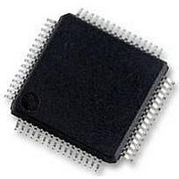
UPD78F0890GK(A)-GAJ-AX NEC, UPD78F0890GK(A)-GAJ-AX Datasheet - Page 612

UPD78F0890GK(A)-GAJ-AX
Manufacturer Part Number
UPD78F0890GK(A)-GAJ-AX
Description
8BIT MCU, 128K FLASH, 7K RAM, LQFP
Manufacturer
NEC
Datasheet
1.UPD78F0890GKA-GAJ-AX.pdf
(732 pages)
Specifications of UPD78F0890GK(A)-GAJ-AX
Controller Family/series
UPD78F
No. Of I/o's
55
Ram Memory Size
7KB
Cpu Speed
20MHz
No. Of Timers
10
No. Of Pwm
RoHS Compliant
Core Size
8bit
Program Memory Size
128KB
Oscillator Type
External, Internal
- Current page: 612 of 732
- Download datasheet (4Mb)
24.7.3 Selecting communication mode
dedicated flash memory programming mode is entered. These FLMD0 pulses are generated by the flash memory
programmer.
Notes 1. Selection items for Standard settings on GUI of the flash memory programmer.
Caution When UART60 is selected, the receive clock is calculated based on the reset command sent from
Remark f
612
UART
(UART60)
3-wire serial I/O
(CSI10)
Communication
In the 78K0/FE2, a communication mode is selected by inputting pulses (up to 8 pulses) to the FLMD0 pin after the
The following table shows the relationship between the number of pulses and communication modes.
Mode
2. Because factors other than the baud rate error, such as the signal waveform slew, also affect UART
3. The possible setting range differs depending on the voltage. For details, refer to the chapter of electrical
the dedicated flash memory programmer after the FLMD0 pulse has been received.
f
f
X
EXCLK
RH
communication, thoroughly evaluate the slew as well as the baud rate error.
specifications.
:
:
: External main system clock
X1 clock
Internal high-speed oscillation clock
UART-Ext-Osc
UART-Ext-FP4CK
CSI-Internal-Osc
Port
115200 bps
2.4 kHz to
2.5 MHz
Table 24-7. Communication Modes
Standard Setting
Speed
CHAPTER 24 FLASH MEMORY
User’s Manual U17554EJ4V0UD
Note 2
2 to 20 MHz
Note 1
Frequency
−
Note 3
1.0
Multiply
Rate
TxD60,
RxD60
SO10, SI10,
SCK10
Pins Used
Peripheral
f
f
f
X
EXCLK
RH
Clock
Number of
FLMD0
Pulses
0
3
8
Related parts for UPD78F0890GK(A)-GAJ-AX
Image
Part Number
Description
Manufacturer
Datasheet
Request
R

Part Number:
Description:
16/8 bit single-chip microcomputer
Manufacturer:
NEC
Datasheet:

Part Number:
Description:
Dual audio power amp circuit
Manufacturer:
NEC
Datasheet:

Part Number:
Description:
Dual comparator
Manufacturer:
NEC
Datasheet:

Part Number:
Description:
MOS type composite field effect transistor
Manufacturer:
NEC
Datasheet:

Part Number:
Description:
50 V/100 mA FET array incorporating 2 N-ch MOSFETs
Manufacturer:
NEC
Datasheet:

Part Number:
Description:
6-pin small MM high-frequency double transistor
Manufacturer:
NEC
Datasheet:

Part Number:
Description:
6-pin small MM high-frequency double transistor
Manufacturer:
NEC
Datasheet:

Part Number:
Description:
6-pin small MM high-frequency double transistor
Manufacturer:
NEC
Datasheet:

Part Number:
Description:
6-pin small MM high-frequency double transistor
Manufacturer:
NEC
Datasheet:

Part Number:
Description:
Twin transistors equipped with different model chips(6P small MM)
Manufacturer:
NEC
Datasheet:

Part Number:
Description:
Bipolar analog integrated circuit
Manufacturer:
NEC
Datasheet:


