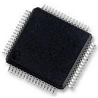
UPD78F0890GK(A)-GAJ-AX NEC, UPD78F0890GK(A)-GAJ-AX Datasheet - Page 373

UPD78F0890GK(A)-GAJ-AX
Manufacturer Part Number
UPD78F0890GK(A)-GAJ-AX
Description
8BIT MCU, 128K FLASH, 7K RAM, LQFP
Manufacturer
NEC
Datasheet
1.UPD78F0890GKA-GAJ-AX.pdf
(732 pages)
Specifications of UPD78F0890GK(A)-GAJ-AX
Controller Family/series
UPD78F
No. Of I/o's
55
Ram Memory Size
7KB
Cpu Speed
20MHz
No. Of Timers
10
No. Of Pwm
RoHS Compliant
Core Size
8bit
Program Memory Size
128KB
Oscillator Type
External, Internal
- Current page: 373 of 732
- Download datasheet (4Mb)
CHAPTER 15 SERIAL INTERFACES CSI10 AND CSI11
(3) Timing of output to SO1n pin (first bit)
When communication is started, the value of transmit buffer register 1n (SOTB1n) is output from the SO1n pin.
The output operation of the first bit at this time is described below.
Figure 15-12. Output Operation of First Bit (1/2)
(a) Type 1: CKP1n = 0, DAP1n = 0
SCK1n
Writing to SOTB1n or
reading from SIO1n
SOTB1n
SIO1n
Output latch
First bit
2nd bit
SO1n
(b) Type 3: CKP1n = 1, DAP1n = 0
SCK1n
Writing to SOTB1n or
reading from SIO1n
SOTB1n
SIO1n
Output latch
SO1n
First bit
2nd bit
The first bit is directly latched by the SOTB1n register to the output latch at the falling (or rising) edge of SCK1n,
and output from the SO1n pin via an output selector. Then, the value of the SOTB1n register is transferred to the
SIO1n register at the next rising (or falling) edge of SCK1n, and shifted one bit. At the same time, the first bit of
the receive data is stored in the SIO1n register via the SI1n pin.
The second and subsequent bits are latched by the SIO1n register to the output latch at the next falling (or rising)
edge of SCK1n, and the data is output from the SO1n pin.
Remark n = 0, 1
373
User’s Manual U17554EJ4V0UD
Related parts for UPD78F0890GK(A)-GAJ-AX
Image
Part Number
Description
Manufacturer
Datasheet
Request
R

Part Number:
Description:
16/8 bit single-chip microcomputer
Manufacturer:
NEC
Datasheet:

Part Number:
Description:
Dual audio power amp circuit
Manufacturer:
NEC
Datasheet:

Part Number:
Description:
Dual comparator
Manufacturer:
NEC
Datasheet:

Part Number:
Description:
MOS type composite field effect transistor
Manufacturer:
NEC
Datasheet:

Part Number:
Description:
50 V/100 mA FET array incorporating 2 N-ch MOSFETs
Manufacturer:
NEC
Datasheet:

Part Number:
Description:
6-pin small MM high-frequency double transistor
Manufacturer:
NEC
Datasheet:

Part Number:
Description:
6-pin small MM high-frequency double transistor
Manufacturer:
NEC
Datasheet:

Part Number:
Description:
6-pin small MM high-frequency double transistor
Manufacturer:
NEC
Datasheet:

Part Number:
Description:
6-pin small MM high-frequency double transistor
Manufacturer:
NEC
Datasheet:

Part Number:
Description:
Twin transistors equipped with different model chips(6P small MM)
Manufacturer:
NEC
Datasheet:

Part Number:
Description:
Bipolar analog integrated circuit
Manufacturer:
NEC
Datasheet:


