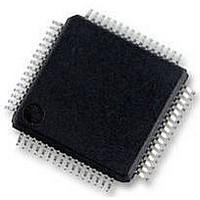
UPD78F0890GK(A)-GAJ-AX NEC, UPD78F0890GK(A)-GAJ-AX Datasheet - Page 724

UPD78F0890GK(A)-GAJ-AX
Manufacturer Part Number
UPD78F0890GK(A)-GAJ-AX
Description
8BIT MCU, 128K FLASH, 7K RAM, LQFP
Manufacturer
NEC
Datasheet
1.UPD78F0890GKA-GAJ-AX.pdf
(732 pages)
Specifications of UPD78F0890GK(A)-GAJ-AX
Controller Family/series
UPD78F
No. Of I/o's
55
Ram Memory Size
7KB
Cpu Speed
20MHz
No. Of Timers
10
No. Of Pwm
RoHS Compliant
Core Size
8bit
Program Memory Size
128KB
Oscillator Type
External, Internal
- Current page: 724 of 732
- Download datasheet (4Mb)
724
3rd
Edition
• Change of Figure 13-4 and Note
• Change of Figure 14-2 and explanation
Change of explanation and Caution in 9.2 (1) 8-bit timer H compare register 0n (CMP0n)
Change of 9.2 (2) 8-bit timer H compare register 1n (CMP1n)
Change of Caution 1 in Figure 9-5. Format of 8-Bit Timer H Mode Register 0 (TMHMD0)
Change of Figure 9-6. Format of 8-Bit Timer H Mode Register 1 (TMHMD1)
Change of Caution 1 in Figure 9-6. Format of 8-Bit Timer H Mode Register 1 (TMHMD1)
Change of Figure 9-7. Format of 8-Bit Timer H Carrier Control Register 1 (TMCYC1)
Change of WTM0 bit in Figure 10-2. Format of Watch Timer Operation Mode Register (WTM)
Change of explanation in 10.4.1 Watch timer operation
Change of Table 10-4. Watch Timer Interrupt Time
Change of Figure 10-3. Operation Timing of Watch Timer/Interval Timer
Change of explanation in 11.1 Functions of Watchdog Timer
Change of explanation in Table 11-2. Setting of Option Bytes and Watchdog Timer and Figure 11-1. Block
Diagram of Watchdog Timer
Change of explanation in 11.4.1 Controlling operation of watchdog timer
Change of Caution 4 and 5 in 11.4.1 Controlling operation of watchdog timer
Change of Caution 2 in Table 11-3. Setting of Overflow Time of Watchdog Timer
Change of explanation in 11.4.3 Setting window open period of watchdog timer
Change of Caution 2 in Table 11-4. Setting Window Open Period of Watchdog Timer
Addition of Note1, Caution1 and 2 in Figure 12-2. Format of Clock Output Selection Register (CKS)
Change of explanation in 13.2 (2) Sample & hold circuit, (3) Series resistor string, (4) Voltage comparator and
(5) Successive approximation register (SAR)
Change of explanation in 13.2 (8) Controller
Change of Note 2 in Figure 13-3. Format of A/D Converter Mode Register (ADM)
Change of Table 13-1. Settings of ADCS and ADCE
Figure 13-4. Timing Chart When Comparator Is Used
Change of (1), (2) and Caution 1 and Addition of Caution 4 in Table 13-2. A/D Conversion Time Selection
Change of Figure 13-8. Format of Analog Input Channel Specification Register (ADS)
Change of explanation and Caution 1 in 13.3 (5) A/D port configuration register (ADPC)
Change of Figure 13-9. Format of A/D Port Configuration Register (ADPC)
Addition of explanation in 13.3 (6) Port mode register 8 (PM8) and (7) Port mode register 9 (PM9)
Change of Table 13-3. Setting Functions of P80/ANI0 to P87/ANI7, P90/ANI8 to P93/ANI11 Pins
Change of 13.4.1 Basic operations of A/D converter
Change of explanation in 13.4.3 (1) A/D conversion operation
Change of 13.6 Cautions for A/D Converter
Change of explanation and Addition of Caution 3 to 5 in 14.1 (2) Asynchronous serial interface (UART) mode
Change of Figure 14-1. LIN Transmission Operation
Figure 14-2. LIN Reception Operation
Addition of Figure 14-4. Port Configuration for LIN Reception Operation (UART61)
Addition of Caution 3 in 14.2 (3) Transmit buffer register 6n (TXB6n)
Change of Note 1 in Figure 14-7. Format of Asynchronous Serial Interface Operation Mode Register 60
(ASIM60) (1/2)
APPENDIX D REVISION HISTORY
User’s Manual U17554EJ4V0UD
Description
(3/9)
Related parts for UPD78F0890GK(A)-GAJ-AX
Image
Part Number
Description
Manufacturer
Datasheet
Request
R

Part Number:
Description:
16/8 bit single-chip microcomputer
Manufacturer:
NEC
Datasheet:

Part Number:
Description:
Dual audio power amp circuit
Manufacturer:
NEC
Datasheet:

Part Number:
Description:
Dual comparator
Manufacturer:
NEC
Datasheet:

Part Number:
Description:
MOS type composite field effect transistor
Manufacturer:
NEC
Datasheet:

Part Number:
Description:
50 V/100 mA FET array incorporating 2 N-ch MOSFETs
Manufacturer:
NEC
Datasheet:

Part Number:
Description:
6-pin small MM high-frequency double transistor
Manufacturer:
NEC
Datasheet:

Part Number:
Description:
6-pin small MM high-frequency double transistor
Manufacturer:
NEC
Datasheet:

Part Number:
Description:
6-pin small MM high-frequency double transistor
Manufacturer:
NEC
Datasheet:

Part Number:
Description:
6-pin small MM high-frequency double transistor
Manufacturer:
NEC
Datasheet:

Part Number:
Description:
Twin transistors equipped with different model chips(6P small MM)
Manufacturer:
NEC
Datasheet:

Part Number:
Description:
Bipolar analog integrated circuit
Manufacturer:
NEC
Datasheet:


