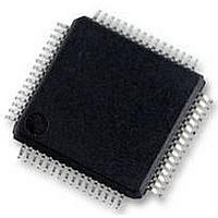
UPD78F0890GK(A)-GAJ-AX NEC, UPD78F0890GK(A)-GAJ-AX Datasheet - Page 609

UPD78F0890GK(A)-GAJ-AX
Manufacturer Part Number
UPD78F0890GK(A)-GAJ-AX
Description
8BIT MCU, 128K FLASH, 7K RAM, LQFP
Manufacturer
NEC
Datasheet
1.UPD78F0890GKA-GAJ-AX.pdf
(732 pages)
Specifications of UPD78F0890GK(A)-GAJ-AX
Controller Family/series
UPD78F
No. Of I/o's
55
Ram Memory Size
7KB
Cpu Speed
20MHz
No. Of Timers
10
No. Of Pwm
RoHS Compliant
Core Size
8bit
Program Memory Size
128KB
Oscillator Type
External, Internal
- Current page: 609 of 732
- Download datasheet (4Mb)
24.6.3 RESET pin
the reset signal generator on the board, signal collision takes place. To prevent this collision, isolate the connection
with the reset signal generator.
memory will not be correctly programmed. Do not input any signal other than the reset signal of the dedicated flash
memory programmer.
24.6.4 Port pins
same status as that immediately after reset. If external devices connected to the ports do not recognize the port
status immediately after reset, the port pin must be connected to V
24.6.5 REGC pin
operation.
24.6.6 Other signal pins
If the reset signal of the dedicated flash memory programmer is connected to the RESET pin that is connected to
If the reset signal is input from the user system while the flash memory programming mode is set, the flash
When the flash memory programming mode is set, all the pins not used for flash memory programming enter the
Connect the REGC pin to GND via a capacitor (0.47 to 1
Connect X1 and X2 in the same status as in the normal operation mode when using the on-board clock.
To input the operating clock from the dedicated flash memory programmer, however, connect as follows.
• PG-FP4, FL-PR4:
• PG-FPL3, FP-LITE3:
Cautions 1. Only the internal high-speed oscillation clock (f
2. Only the X1 clock (f
3. Connect P31/INTP2/TI002 and P121/X1 as follows when writing the flash memory with a
used.
flash memory programmer.
The above connection is not necessary when writing the flash memory by means of self
programming.
• P31/INTP2/TI002: Connect to EV
• P121/X1: When using this pin as a port, connect it to V
78K0/FE2
RESET
Connect CLK of the programmer to EXCLK/X2/P122.
Connect CLK of the programmer and X1/P121, and connect its inverted signal to
X2/EXCLK/P122.
In the flash memory programming mode, the signal output by the reset
signal generator collides with the signal output by the dedicated flash
memory programmer. Therefore, isolate the signal of the reset signal
generator.
recommended) (in the input mode) or leave it open (in the output mode).
Figure 24-11. Signal Collision (RESET Pin)
Signal collision
X
) or external main system clock (f
CHAPTER 24 FLASH MEMORY
User’s Manual U17554EJ4V0UD
Reset signal generator
SS
Dedicated flash memory
programmer connection signal
via a resistor (10 kΩ: recommended).
μ
Output pin
F: recommended) in the same manner as during normal
DD
or V
RH
) can be used when CSI10 is used.
SS
via a resistor.
EXCLK
) can be used when UART60 is
SS
via a resistor (10 kΩ:
609
Related parts for UPD78F0890GK(A)-GAJ-AX
Image
Part Number
Description
Manufacturer
Datasheet
Request
R

Part Number:
Description:
16/8 bit single-chip microcomputer
Manufacturer:
NEC
Datasheet:

Part Number:
Description:
Dual audio power amp circuit
Manufacturer:
NEC
Datasheet:

Part Number:
Description:
Dual comparator
Manufacturer:
NEC
Datasheet:

Part Number:
Description:
MOS type composite field effect transistor
Manufacturer:
NEC
Datasheet:

Part Number:
Description:
50 V/100 mA FET array incorporating 2 N-ch MOSFETs
Manufacturer:
NEC
Datasheet:

Part Number:
Description:
6-pin small MM high-frequency double transistor
Manufacturer:
NEC
Datasheet:

Part Number:
Description:
6-pin small MM high-frequency double transistor
Manufacturer:
NEC
Datasheet:

Part Number:
Description:
6-pin small MM high-frequency double transistor
Manufacturer:
NEC
Datasheet:

Part Number:
Description:
6-pin small MM high-frequency double transistor
Manufacturer:
NEC
Datasheet:

Part Number:
Description:
Twin transistors equipped with different model chips(6P small MM)
Manufacturer:
NEC
Datasheet:

Part Number:
Description:
Bipolar analog integrated circuit
Manufacturer:
NEC
Datasheet:


