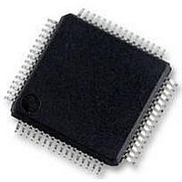
UPD78F0890GK(A)-GAJ-AX NEC, UPD78F0890GK(A)-GAJ-AX Datasheet - Page 98

UPD78F0890GK(A)-GAJ-AX
Manufacturer Part Number
UPD78F0890GK(A)-GAJ-AX
Description
8BIT MCU, 128K FLASH, 7K RAM, LQFP
Manufacturer
NEC
Datasheet
1.UPD78F0890GKA-GAJ-AX.pdf
(732 pages)
Specifications of UPD78F0890GK(A)-GAJ-AX
Controller Family/series
UPD78F
No. Of I/o's
55
Ram Memory Size
7KB
Cpu Speed
20MHz
No. Of Timers
10
No. Of Pwm
RoHS Compliant
Core Size
8bit
Program Memory Size
128KB
Oscillator Type
External, Internal
- Current page: 98 of 732
- Download datasheet (4Mb)
<R>
5.2.3 Port 3
using port mode register 3 (PM3). When used as an input port, use of an on-chip pull-up resistor can be specified in
1-bit units by pull-up resistor option register 3 (PU3).
98
Port 3 is a 4-bit I/O port with an output latch. Port 3 can be set to the input mode or output mode in 1-bit units
This port can also be used for external interrupt request input and timer I/O.
Reset signal generation sets port 3 to input mode.
Figures 5-7 and 5-8 show block diagrams of port 3.
Cautions 1. Be sure to pull the P31 pin down before a reset release, to prevent malfunction.
Remark P31/INTP2/TI002 and P32/INTP3/TI012/TO02 can be used for on-chip debug mode setting when the
WR
P3:
PU3:
PM3:
RD:
WR××: Write signal
WR
WR
RD
PORT
PM
PU
on-chip debug function is used. For details, refer to CHAPTER 25 ON-CHIP DEBUG FUNCTION.
2. Connect P31/TI002/INTP2 as follows when writing the flash memory with a flash programmer.
- P31/TI002/INTP2: Connect to EV
The above connection is not necessary when writing the flash memory by means of self
programming.
Port register 3
Pull-up resistor option register 3
Port mode register 3
Read signal
PM30, PM31
PU30, PU31
Output latch
(P30, P31)
Alternate
function
PM3
PU3
P3
Figure 5-7. Block Diagram of P30 and P31
CHAPTER 5 PORT FUNCTIONS
User’s Manual U17554EJ4V0UD
SS
via a resistor (10 kΩ: recommended).
EV
DD
P-ch
P30/INTP1,
P31/INTP2/TI002
Related parts for UPD78F0890GK(A)-GAJ-AX
Image
Part Number
Description
Manufacturer
Datasheet
Request
R

Part Number:
Description:
16/8 bit single-chip microcomputer
Manufacturer:
NEC
Datasheet:

Part Number:
Description:
Dual audio power amp circuit
Manufacturer:
NEC
Datasheet:

Part Number:
Description:
Dual comparator
Manufacturer:
NEC
Datasheet:

Part Number:
Description:
MOS type composite field effect transistor
Manufacturer:
NEC
Datasheet:

Part Number:
Description:
50 V/100 mA FET array incorporating 2 N-ch MOSFETs
Manufacturer:
NEC
Datasheet:

Part Number:
Description:
6-pin small MM high-frequency double transistor
Manufacturer:
NEC
Datasheet:

Part Number:
Description:
6-pin small MM high-frequency double transistor
Manufacturer:
NEC
Datasheet:

Part Number:
Description:
6-pin small MM high-frequency double transistor
Manufacturer:
NEC
Datasheet:

Part Number:
Description:
6-pin small MM high-frequency double transistor
Manufacturer:
NEC
Datasheet:

Part Number:
Description:
Twin transistors equipped with different model chips(6P small MM)
Manufacturer:
NEC
Datasheet:

Part Number:
Description:
Bipolar analog integrated circuit
Manufacturer:
NEC
Datasheet:


