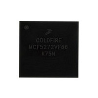
MCF5272VF66 Freescale, MCF5272VF66 Datasheet - Page 123

MCF5272VF66
Manufacturer Part Number
MCF5272VF66
Description
Manufacturer
Freescale
Datasheet
1.MCF5272VF66.pdf
(544 pages)
Specifications of MCF5272VF66
Family Name
MCF5xxx
Device Core
ColdFire
Device Core Size
32b
Frequency (max)
66MHz
Instruction Set Architecture
RISC
Supply Voltage 1 (typ)
3.3V
Operating Temp Range
0C to 70C
Operating Temperature Classification
Commercial
Mounting
Surface Mount
Pin Count
196
Package Type
MA-BGA
Lead Free Status / RoHS Status
Not Compliant
Available stocks
Company
Part Number
Manufacturer
Quantity
Price
Company:
Part Number:
MCF5272VF66
Manufacturer:
HYNIX
Quantity:
19
Company:
Part Number:
MCF5272VF66
Manufacturer:
FREESCAL
Quantity:
885
Company:
Part Number:
MCF5272VF66
Manufacturer:
Freescale Semiconductor
Quantity:
10 000
Part Number:
MCF5272VF66
Manufacturer:
FREESCALE
Quantity:
20 000
Company:
Part Number:
MCF5272VF66J
Manufacturer:
Freescale
Quantity:
256
Company:
Part Number:
MCF5272VF66J
Manufacturer:
Freescale Semiconductor
Quantity:
10 000
Company:
Part Number:
MCF5272VF66R2
Manufacturer:
Freescale Semiconductor
Quantity:
10 000
Company:
Part Number:
MCF5272VF66R2J
Manufacturer:
Freescale Semiconductor
Quantity:
10 000
- Current page: 123 of 544
- Download datasheet (7Mb)
Another example of a variant branch instruction would be a JMP (A0) instruction.
the PST and DDATA outputs that indicate when a JMP (A0) executed, assuming the CSR was programmed
to display the lower 2 bytes of an address.
PST of 0x5 indicates a taken branch and the marker value 0x9 indicates a 2-byte address. Thus, the
subsequent 4 nibbles of DDATA display the lower 2 bytes of address register A0 in
least-to-most-significant nibble order. The PST output after the JMP instruction completes depends on the
target instruction. The PST can continue with the next instruction before the address has completely
displayed on DDATA because of the DDATA FIFO. If the FIFO is full and the next instruction has captured
values to display on DDATA, the pipeline stalls (PST = 0x0) until space is available in the FIFO.
5.4
In addition to the existing BDM commands that provide access to the processor’s registers and the memory
subsystem, the debug module contains nine registers to support the required functionality. These registers
are also accessible from the processor’s supervisor programming model by executing the WDEBUG
instruction (write only). Thus, the breakpoint hardware in the debug module can be read or written by the
external development system using the debug serial interface or by the operating system running on the
processor core. Software is responsible for guaranteeing that accesses to these resources are serialized and
logically consistent. Hardware provides a locking mechanism in the CSR to allow the external
development system to disable any attempted writes by the processor to the breakpoint registers (setting
CSR[IPW]). BDM commands must not be issued if the MCF5272 is using the WDEBUG instruction to
access debug module registers or the resulting behavior is undefined.
These registers, shown in
implemented bits.
Freescale Semiconductor
PSTCLK
DDATA
PST
Programming Model
MCF5272 ColdFire
Figure 5-3. Example JMP Instruction Output on PST/DDATA
0x5
0x0
Figure
5-4, are treated as 32-bit quantities, regardless of the number of
0x9
0x0
®
Integrated Microprocessor User’s Manual, Rev. 3
default
A[3:0]
default
A[7:4]
A[11:8]
default
Figure 5-3
A[15:12]
default
shows when
Debug Support
5-5
Related parts for MCF5272VF66
Image
Part Number
Description
Manufacturer
Datasheet
Request
R
Part Number:
Description:
Mcf5272 Coldfire Integrated Microprocessor User
Manufacturer:
Freescale Semiconductor, Inc
Datasheet:

Part Number:
Description:
MCF5272 Interrupt Service Routine for the Physical Layer Interface Controller
Manufacturer:
Freescale Semiconductor / Motorola
Datasheet:

Part Number:
Description:
TOWER ELEVATOR BOARDS HARDWARE
Manufacturer:
Freescale Semiconductor
Datasheet:

Part Number:
Description:
TOWER SERIAL I/O HARDWARE
Manufacturer:
Freescale Semiconductor
Datasheet:

Part Number:
Description:
LCD MODULE FOR TWR SYSTEM
Manufacturer:
Freescale Semiconductor
Datasheet:

Part Number:
Description:
DAUGHTER LCD WVGA I.MX51
Manufacturer:
Freescale Semiconductor
Datasheet:

Part Number:
Description:
TOWER SYSTEM BOARD MPC5125
Manufacturer:
Freescale Semiconductor
Datasheet:

Part Number:
Description:
KIT EVALUATION I.MX51
Manufacturer:
Freescale Semiconductor
Datasheet:

Part Number:
Description:
KIT DEVELOPMENT WINCE IMX25
Manufacturer:
Freescale Semiconductor
Datasheet:

Part Number:
Description:
TOWER SYSTEM KIT MPC5125
Manufacturer:
Freescale Semiconductor
Datasheet:

Part Number:
Description:
TOWER SYSTEM BOARD K40X256
Manufacturer:
Freescale Semiconductor
Datasheet:

Part Number:
Description:
TOWER SYSTEM KIT K40X256
Manufacturer:
Freescale Semiconductor
Datasheet:

Part Number:
Description:
Microcontrollers (MCU) MX28 PLATFORM DEV KIT
Manufacturer:
Freescale Semiconductor
Datasheet:

Part Number:
Description:
MCU, MPU & DSP Development Tools IAR KickStart Kit for Kinetis K60
Manufacturer:
Freescale Semiconductor
Datasheet:

Part Number:
Description:
24BIT HDMI MX535/08
Manufacturer:
Freescale Semiconductor
Datasheet:


