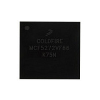
MCF5272VF66 Freescale, MCF5272VF66 Datasheet - Page 432

MCF5272VF66
Manufacturer Part Number
MCF5272VF66
Description
Manufacturer
Freescale
Datasheet
1.MCF5272VF66.pdf
(544 pages)
Specifications of MCF5272VF66
Family Name
MCF5xxx
Device Core
ColdFire
Device Core Size
32b
Frequency (max)
66MHz
Instruction Set Architecture
RISC
Supply Voltage 1 (typ)
3.3V
Operating Temp Range
0C to 70C
Operating Temperature Classification
Commercial
Mounting
Surface Mount
Pin Count
196
Package Type
MA-BGA
Lead Free Status / RoHS Status
Not Compliant
Available stocks
Company
Part Number
Manufacturer
Quantity
Price
Company:
Part Number:
MCF5272VF66
Manufacturer:
HYNIX
Quantity:
19
Company:
Part Number:
MCF5272VF66
Manufacturer:
FREESCAL
Quantity:
885
Company:
Part Number:
MCF5272VF66
Manufacturer:
Freescale Semiconductor
Quantity:
10 000
Part Number:
MCF5272VF66
Manufacturer:
FREESCALE
Quantity:
20 000
Company:
Part Number:
MCF5272VF66J
Manufacturer:
Freescale
Quantity:
256
Company:
Part Number:
MCF5272VF66J
Manufacturer:
Freescale Semiconductor
Quantity:
10 000
Company:
Part Number:
MCF5272VF66R2
Manufacturer:
Freescale Semiconductor
Quantity:
10 000
Company:
Part Number:
MCF5272VF66R2J
Manufacturer:
Freescale Semiconductor
Quantity:
10 000
- Current page: 432 of 544
- Download datasheet (7Mb)
Signal Descriptions
19.6.4
Assertion of the transfer acknowledge (TA/PB5) input terminates an external bus cycle. It is enabled on a
per chip select basis by programming the wait state field to 0x1F in the corresponding chip select option
register (CSORn[WS]). This pin requires a 4.7-K¾ pull-up resistor or external logic that drives inactive
high.
TA must always be returned high before it can be detected again. Asserting TA into the next bus cycle has
no effect and does not terminate the bus cycle.
19.6.5
HiZ is a test signal. When it is connected to GND during reset, all output pins are driven to high impedance.
A 4.7-K¾ pullup resistor should be connected to this signal if the Hi-Z function is not used. Hi-Z
configuration input is sampled on the rising edge of Reset Output (RSTO).
19.6.6
Bypass is a Freescale test mode signal. This signal should be left unconnected.
19.6.7
RAS0 is the SDRAM row address strobe output.
19.6.8
CAS0 is the SDRAM column address strobe output.
19.6.9
The SDRAM clock output (SDCLK) is the same frequency as the CPU clock.
19.6.10 SDRAM Write Enable (SDWE)
This output is the SDRAM write enable.
19.6.11 SDRAM Clock Enable (SDCLKE)
This output is the SDRAM clock enable.
19-22
Transfer Acknowledge (TA/PB5)
Hi-Z
Bypass
SDRAM Row Address Strobe (RAS0)
SDRAM Column Address Strobe (CAS0)
SDRAM Clock (SDCLK)
Even though EBI modes set to SDRAM require setting the wait state field
in the chip select option register to 31, a low signal should never be applied
to TA during such accesses. For SDRAM accesses the bus cycle is
terminated internally by circuitry in the SDRAM module.
MCF5272 ColdFire
®
Integrated Microprocessor User’s Manual, Rev. 3
NOTE:
Freescale Semiconductor
Related parts for MCF5272VF66
Image
Part Number
Description
Manufacturer
Datasheet
Request
R
Part Number:
Description:
Mcf5272 Coldfire Integrated Microprocessor User
Manufacturer:
Freescale Semiconductor, Inc
Datasheet:

Part Number:
Description:
MCF5272 Interrupt Service Routine for the Physical Layer Interface Controller
Manufacturer:
Freescale Semiconductor / Motorola
Datasheet:

Part Number:
Description:
TOWER ELEVATOR BOARDS HARDWARE
Manufacturer:
Freescale Semiconductor
Datasheet:

Part Number:
Description:
TOWER SERIAL I/O HARDWARE
Manufacturer:
Freescale Semiconductor
Datasheet:

Part Number:
Description:
LCD MODULE FOR TWR SYSTEM
Manufacturer:
Freescale Semiconductor
Datasheet:

Part Number:
Description:
DAUGHTER LCD WVGA I.MX51
Manufacturer:
Freescale Semiconductor
Datasheet:

Part Number:
Description:
TOWER SYSTEM BOARD MPC5125
Manufacturer:
Freescale Semiconductor
Datasheet:

Part Number:
Description:
KIT EVALUATION I.MX51
Manufacturer:
Freescale Semiconductor
Datasheet:

Part Number:
Description:
KIT DEVELOPMENT WINCE IMX25
Manufacturer:
Freescale Semiconductor
Datasheet:

Part Number:
Description:
TOWER SYSTEM KIT MPC5125
Manufacturer:
Freescale Semiconductor
Datasheet:

Part Number:
Description:
TOWER SYSTEM BOARD K40X256
Manufacturer:
Freescale Semiconductor
Datasheet:

Part Number:
Description:
TOWER SYSTEM KIT K40X256
Manufacturer:
Freescale Semiconductor
Datasheet:

Part Number:
Description:
Microcontrollers (MCU) MX28 PLATFORM DEV KIT
Manufacturer:
Freescale Semiconductor
Datasheet:

Part Number:
Description:
MCU, MPU & DSP Development Tools IAR KickStart Kit for Kinetis K60
Manufacturer:
Freescale Semiconductor
Datasheet:

Part Number:
Description:
24BIT HDMI MX535/08
Manufacturer:
Freescale Semiconductor
Datasheet:


