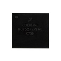
MCF5272VF66 Freescale, MCF5272VF66 Datasheet - Page 353

MCF5272VF66
Manufacturer Part Number
MCF5272VF66
Description
Manufacturer
Freescale
Datasheet
1.MCF5272VF66.pdf
(544 pages)
Specifications of MCF5272VF66
Family Name
MCF5xxx
Device Core
ColdFire
Device Core Size
32b
Frequency (max)
66MHz
Instruction Set Architecture
RISC
Supply Voltage 1 (typ)
3.3V
Operating Temp Range
0C to 70C
Operating Temperature Classification
Commercial
Mounting
Surface Mount
Pin Count
196
Package Type
MA-BGA
Lead Free Status / RoHS Status
Not Compliant
Available stocks
Company
Part Number
Manufacturer
Quantity
Price
Company:
Part Number:
MCF5272VF66
Manufacturer:
HYNIX
Quantity:
19
Company:
Part Number:
MCF5272VF66
Manufacturer:
FREESCAL
Quantity:
885
Company:
Part Number:
MCF5272VF66
Manufacturer:
Freescale Semiconductor
Quantity:
10 000
Part Number:
MCF5272VF66
Manufacturer:
FREESCALE
Quantity:
20 000
Company:
Part Number:
MCF5272VF66J
Manufacturer:
Freescale
Quantity:
256
Company:
Part Number:
MCF5272VF66J
Manufacturer:
Freescale Semiconductor
Quantity:
10 000
Company:
Part Number:
MCF5272VF66R2
Manufacturer:
Freescale Semiconductor
Quantity:
10 000
Company:
Part Number:
MCF5272VF66R2J
Manufacturer:
Freescale Semiconductor
Quantity:
10 000
- Current page: 353 of 544
- Download datasheet (7Mb)
14.5.7
The command RAM is accessed using the upper byte of QDR. The QSPI cannot modify information in
command RAM.
There are 16 bytes in the command RAM. Each byte is divided into two fields. The chip select field enables
external peripherals for transfer. The command field provides transfer operations.
Figure 14-11
Table 14-7
1
Freescale Semiconductor
In order to keep the chip setects asserted for all transfers, the QWR[CSIV] bit must be set to control the level that the chip
selects return to after the first transfer.
11–8
Bits
7–0
15
14
13
12
Address
Reset
Field
R/W
gives QCR field descriptions.
Command RAM Registers (QCR0–QCR15)
shows the command RAM register.
CONT
QSPI_CS
The command RAM is accessed only using the most significant byte of
QDR and indirect addressing based on QAR[ADDR].
15
CONT
BITSE
Name
DSCK
DT
—
BITSE
MCF5272 ColdFire
14
Figure 14-11. Command RAM Registers (QCR0–QCR15)
Continuous.
0 Chip selects return to inactive level defined by QWR[CSIV] when transfer is complete.
1 Chip selects remain asserted between transfers for a transfer of up to 16 words of data.
Bits per transfer enable.
0 Eight bits
1 Number of bits set in QMR[BITS]
Delay after transfer enable.
0 Default reset value.
1 The QSPI provides a variable delay at the end of serial transfer to facilitate interfacing with
Chip select to QSPI_CLK delay enable.
0 Chip select valid to QSPI_CLK transition is one-half QSPI_CLK period.
1 QDLYR[QCD] specifies the delay from QSPI_CS valid to QSPI_CLK.
Peripheral chip selects. Used to select an external device for serial data transfer. More than one
chip select may be active at once, and more than one device can be connected to each chip
select. Bits 11–8 map directly to QSPI_CS[3:0], respectively. If it is desired to use those bits as
a chip select value, then an external demultiplexor must be connected to the QSPI_CS[3:0] pins.
Reserved, should be cleared.
peripherals that have a latency requirement. The delay between transfers is determined by
QDLYR[DTL].
DT
13
Table 14-7. QCR0–QCR15 Field Descriptions
DSCK
12
®
Integrated Microprocessor User’s Manual, Rev. 3
11
NOTE
QSPI_CS
QAR[ADDR]
Write Only
Undefined
Description
8
Queued Serial Peripheral Interface (QSPI) Module
7
–
0
14-15
1
Related parts for MCF5272VF66
Image
Part Number
Description
Manufacturer
Datasheet
Request
R
Part Number:
Description:
Mcf5272 Coldfire Integrated Microprocessor User
Manufacturer:
Freescale Semiconductor, Inc
Datasheet:

Part Number:
Description:
MCF5272 Interrupt Service Routine for the Physical Layer Interface Controller
Manufacturer:
Freescale Semiconductor / Motorola
Datasheet:

Part Number:
Description:
TOWER ELEVATOR BOARDS HARDWARE
Manufacturer:
Freescale Semiconductor
Datasheet:

Part Number:
Description:
TOWER SERIAL I/O HARDWARE
Manufacturer:
Freescale Semiconductor
Datasheet:

Part Number:
Description:
LCD MODULE FOR TWR SYSTEM
Manufacturer:
Freescale Semiconductor
Datasheet:

Part Number:
Description:
DAUGHTER LCD WVGA I.MX51
Manufacturer:
Freescale Semiconductor
Datasheet:

Part Number:
Description:
TOWER SYSTEM BOARD MPC5125
Manufacturer:
Freescale Semiconductor
Datasheet:

Part Number:
Description:
KIT EVALUATION I.MX51
Manufacturer:
Freescale Semiconductor
Datasheet:

Part Number:
Description:
KIT DEVELOPMENT WINCE IMX25
Manufacturer:
Freescale Semiconductor
Datasheet:

Part Number:
Description:
TOWER SYSTEM KIT MPC5125
Manufacturer:
Freescale Semiconductor
Datasheet:

Part Number:
Description:
TOWER SYSTEM BOARD K40X256
Manufacturer:
Freescale Semiconductor
Datasheet:

Part Number:
Description:
TOWER SYSTEM KIT K40X256
Manufacturer:
Freescale Semiconductor
Datasheet:

Part Number:
Description:
Microcontrollers (MCU) MX28 PLATFORM DEV KIT
Manufacturer:
Freescale Semiconductor
Datasheet:

Part Number:
Description:
MCU, MPU & DSP Development Tools IAR KickStart Kit for Kinetis K60
Manufacturer:
Freescale Semiconductor
Datasheet:

Part Number:
Description:
24BIT HDMI MX535/08
Manufacturer:
Freescale Semiconductor
Datasheet:


