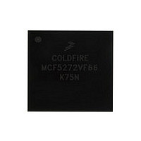
MCF5272VF66 Freescale, MCF5272VF66 Datasheet - Page 135

MCF5272VF66
Manufacturer Part Number
MCF5272VF66
Description
Manufacturer
Freescale
Datasheet
1.MCF5272VF66.pdf
(544 pages)
Specifications of MCF5272VF66
Family Name
MCF5xxx
Device Core
ColdFire
Device Core Size
32b
Frequency (max)
66MHz
Instruction Set Architecture
RISC
Supply Voltage 1 (typ)
3.3V
Operating Temp Range
0C to 70C
Operating Temperature Classification
Commercial
Mounting
Surface Mount
Pin Count
196
Package Type
MA-BGA
Lead Free Status / RoHS Status
Not Compliant
Available stocks
Company
Part Number
Manufacturer
Quantity
Price
Company:
Part Number:
MCF5272VF66
Manufacturer:
HYNIX
Quantity:
19
Company:
Part Number:
MCF5272VF66
Manufacturer:
FREESCAL
Quantity:
885
Company:
Part Number:
MCF5272VF66
Manufacturer:
Freescale Semiconductor
Quantity:
10 000
Part Number:
MCF5272VF66
Manufacturer:
FREESCALE
Quantity:
20 000
Company:
Part Number:
MCF5272VF66J
Manufacturer:
Freescale
Quantity:
256
Company:
Part Number:
MCF5272VF66J
Manufacturer:
Freescale Semiconductor
Quantity:
10 000
Company:
Part Number:
MCF5272VF66R2
Manufacturer:
Freescale Semiconductor
Quantity:
10 000
Company:
Part Number:
MCF5272VF66R2J
Manufacturer:
Freescale Semiconductor
Quantity:
10 000
- Current page: 135 of 544
- Download datasheet (7Mb)
5.5.2
When the CPU is halted and PST reflects the halt status, the development system can send unrestricted
commands to the debug module. The debug module implements a synchronous protocol using two inputs
(DSCLK and DSI) and one output (DSO), where DSO is specified as a delay relative to the rising edge of
the processor clock. See
master and must generate DSCLK.
The serial channel operates at a frequency from DC to 1/5 of the PSTCLK frequency. The channel uses
full-duplex mode, where data is sent and received simultaneously by both master and slave devices. The
transmission consists of 17-bit packets composed of a status/control bit and a 16-bit data word. As shown
in
high; that is, DSI is sampled and DSO is driven.
DSCLK and DSI are synchronized inputs. DSCLK acts as a pseudo clock enable and is sampled on the
rising edge of the processor CLK as well as the DSI. DSO is delayed from the DSCLK-enabled CLK rising
edge (registered after a BDM state machine state change). All events in the debug module’s serial state
machine are based on the processor clock rising edge. DSCLK must also be sampled low (on a positive
edge of CLK) between each bit exchange. The MSB is transferred first. Because DSO changes state based
on an internally-recognized rising edge of DSCLK, DSDO cannot be used to indicate the start of a serial
transfer. The development system must count clock cycles in a given transfer. C1–C4 are described as
follows:
Freescale Semiconductor
Figure
•
•
•
•
C1—First synchronization cycle for DSI (DSCLK is high).
C2—Second synchronization cycle for DSI (DSCLK is high).
C3—BDM state machine changes state depending upon DSI and whether the entire input data
transfer has been transmitted.
C4—DSO changes to next value.
5-12, all state transitions are enabled on a rising edge of the PSTCLK clock when DSCLK is
BDM State
PSTCLK
Machine
BDM Serial Interface
DSCLK
DSO
A not-ready response can be ignored except during a memory-referencing
cycle. Otherwise, the debug module can accept a new serial transfer after 32
processor clock periods.
DSI
MCF5272 ColdFire
Table
5-1. The development system serves as the serial communication channel
Current State
Figure 5-12. BDM Serial Interface Timing
Past
®
Integrated Microprocessor User’s Manual, Rev. 3
C1
Current
C2
NOTE
C3
C4
Next State
Current
Next
Debug Support
5-17
Related parts for MCF5272VF66
Image
Part Number
Description
Manufacturer
Datasheet
Request
R
Part Number:
Description:
Mcf5272 Coldfire Integrated Microprocessor User
Manufacturer:
Freescale Semiconductor, Inc
Datasheet:

Part Number:
Description:
MCF5272 Interrupt Service Routine for the Physical Layer Interface Controller
Manufacturer:
Freescale Semiconductor / Motorola
Datasheet:

Part Number:
Description:
TOWER ELEVATOR BOARDS HARDWARE
Manufacturer:
Freescale Semiconductor
Datasheet:

Part Number:
Description:
TOWER SERIAL I/O HARDWARE
Manufacturer:
Freescale Semiconductor
Datasheet:

Part Number:
Description:
LCD MODULE FOR TWR SYSTEM
Manufacturer:
Freescale Semiconductor
Datasheet:

Part Number:
Description:
DAUGHTER LCD WVGA I.MX51
Manufacturer:
Freescale Semiconductor
Datasheet:

Part Number:
Description:
TOWER SYSTEM BOARD MPC5125
Manufacturer:
Freescale Semiconductor
Datasheet:

Part Number:
Description:
KIT EVALUATION I.MX51
Manufacturer:
Freescale Semiconductor
Datasheet:

Part Number:
Description:
KIT DEVELOPMENT WINCE IMX25
Manufacturer:
Freescale Semiconductor
Datasheet:

Part Number:
Description:
TOWER SYSTEM KIT MPC5125
Manufacturer:
Freescale Semiconductor
Datasheet:

Part Number:
Description:
TOWER SYSTEM BOARD K40X256
Manufacturer:
Freescale Semiconductor
Datasheet:

Part Number:
Description:
TOWER SYSTEM KIT K40X256
Manufacturer:
Freescale Semiconductor
Datasheet:

Part Number:
Description:
Microcontrollers (MCU) MX28 PLATFORM DEV KIT
Manufacturer:
Freescale Semiconductor
Datasheet:

Part Number:
Description:
MCU, MPU & DSP Development Tools IAR KickStart Kit for Kinetis K60
Manufacturer:
Freescale Semiconductor
Datasheet:

Part Number:
Description:
24BIT HDMI MX535/08
Manufacturer:
Freescale Semiconductor
Datasheet:


