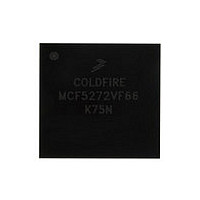
MCF5272VF66 Freescale, MCF5272VF66 Datasheet - Page 299

MCF5272VF66
Manufacturer Part Number
MCF5272VF66
Description
Manufacturer
Freescale
Datasheet
1.MCF5272VF66.pdf
(544 pages)
Specifications of MCF5272VF66
Family Name
MCF5xxx
Device Core
ColdFire
Device Core Size
32b
Frequency (max)
66MHz
Instruction Set Architecture
RISC
Supply Voltage 1 (typ)
3.3V
Operating Temp Range
0C to 70C
Operating Temperature Classification
Commercial
Mounting
Surface Mount
Pin Count
196
Package Type
MA-BGA
Lead Free Status / RoHS Status
Not Compliant
Available stocks
Company
Part Number
Manufacturer
Quantity
Price
Company:
Part Number:
MCF5272VF66
Manufacturer:
HYNIX
Quantity:
19
Company:
Part Number:
MCF5272VF66
Manufacturer:
FREESCAL
Quantity:
885
Company:
Part Number:
MCF5272VF66
Manufacturer:
Freescale Semiconductor
Quantity:
10 000
Part Number:
MCF5272VF66
Manufacturer:
FREESCALE
Quantity:
20 000
Company:
Part Number:
MCF5272VF66J
Manufacturer:
Freescale
Quantity:
256
Company:
Part Number:
MCF5272VF66J
Manufacturer:
Freescale Semiconductor
Quantity:
10 000
Company:
Part Number:
MCF5272VF66R2
Manufacturer:
Freescale Semiconductor
Quantity:
10 000
Company:
Part Number:
MCF5272VF66R2J
Manufacturer:
Freescale Semiconductor
Quantity:
10 000
- Current page: 299 of 544
- Download datasheet (7Mb)
The MCF5272 PLIC provides two sets of D-channel arbitration control pins:
Because pin set 1 connects ports 1, 2, and 3, these ports do not have D-channel arbitration control signals.
13.2
This section describes the GCI/IDL block.
13.2.1
The maximum data rate received for each GCI/IDL port is 144 Kbps: the sum of two 64-Kbps B channels
and one 16-Kbps D-channel. Frames of B
bits). Frames of D-channels are packed together to form bytes. For channels B and D, this requires CPU
service at a 2-KHz rate, because it requires four frames to fill the 32-bit B-channel register and the 8-bit
D-channel register.
The CPU should service the B1 and B2 registers once every 500 μS. Overrun conditions can be avoided
only if the CPU services these registers in a timely manner.
The MCF5272 has 4 GCI/IDL interfaces. Thus the theoretical maximum is twelve 32-bit data registers to
be read. For most applications the typical number is less.
Freescale Semiconductor
•
•
frame sync (offset with respect to the port 1 GCI/IDL block). Port 3 can also have dedicated data
in and data out pins, DIN3 and DOUT3 of pin set 3 (see
Registers
common frame sync and clock, but two sets of serial data-in and data-out pins.
DREQ0 and DGNT0 for pin set 0
DREQ1 and DGNT1 for pin set 1
Demultiplexing
Circuitry
DIN
GCI/IDL Block
GCI/IDL B- and D-Channel Receive Data Registers
DCL
(P0CR–P3CR)”). This allows the MCF5272 to connect to ISDN NT1s that have a
MCF5272 ColdFire
B1 Shift Register
B1 Channel
32
Figure 13-2. GCI/IDL Receive Data Flow
®
Integrated Microprocessor User’s Manual, Rev. 3
1
and B
Internal Bus
B2 Shift Register
2
B2 Channel
channels are packed together to form longwords (32
32
Section 13.5.7, “Port Configuration
D Shift Register
Physical Layer Interface Controller (PLIC)
D Channel
8
13-3
Related parts for MCF5272VF66
Image
Part Number
Description
Manufacturer
Datasheet
Request
R
Part Number:
Description:
Mcf5272 Coldfire Integrated Microprocessor User
Manufacturer:
Freescale Semiconductor, Inc
Datasheet:

Part Number:
Description:
MCF5272 Interrupt Service Routine for the Physical Layer Interface Controller
Manufacturer:
Freescale Semiconductor / Motorola
Datasheet:

Part Number:
Description:
TOWER ELEVATOR BOARDS HARDWARE
Manufacturer:
Freescale Semiconductor
Datasheet:

Part Number:
Description:
TOWER SERIAL I/O HARDWARE
Manufacturer:
Freescale Semiconductor
Datasheet:

Part Number:
Description:
LCD MODULE FOR TWR SYSTEM
Manufacturer:
Freescale Semiconductor
Datasheet:

Part Number:
Description:
DAUGHTER LCD WVGA I.MX51
Manufacturer:
Freescale Semiconductor
Datasheet:

Part Number:
Description:
TOWER SYSTEM BOARD MPC5125
Manufacturer:
Freescale Semiconductor
Datasheet:

Part Number:
Description:
KIT EVALUATION I.MX51
Manufacturer:
Freescale Semiconductor
Datasheet:

Part Number:
Description:
KIT DEVELOPMENT WINCE IMX25
Manufacturer:
Freescale Semiconductor
Datasheet:

Part Number:
Description:
TOWER SYSTEM KIT MPC5125
Manufacturer:
Freescale Semiconductor
Datasheet:

Part Number:
Description:
TOWER SYSTEM BOARD K40X256
Manufacturer:
Freescale Semiconductor
Datasheet:

Part Number:
Description:
TOWER SYSTEM KIT K40X256
Manufacturer:
Freescale Semiconductor
Datasheet:

Part Number:
Description:
Microcontrollers (MCU) MX28 PLATFORM DEV KIT
Manufacturer:
Freescale Semiconductor
Datasheet:

Part Number:
Description:
MCU, MPU & DSP Development Tools IAR KickStart Kit for Kinetis K60
Manufacturer:
Freescale Semiconductor
Datasheet:

Part Number:
Description:
24BIT HDMI MX535/08
Manufacturer:
Freescale Semiconductor
Datasheet:


