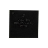
MCF5272VF66 Freescale, MCF5272VF66 Datasheet - Page 189

MCF5272VF66
Manufacturer Part Number
MCF5272VF66
Description
Manufacturer
Freescale
Datasheet
1.MCF5272VF66.pdf
(544 pages)
Specifications of MCF5272VF66
Family Name
MCF5xxx
Device Core
ColdFire
Device Core Size
32b
Frequency (max)
66MHz
Instruction Set Architecture
RISC
Supply Voltage 1 (typ)
3.3V
Operating Temp Range
0C to 70C
Operating Temperature Classification
Commercial
Mounting
Surface Mount
Pin Count
196
Package Type
MA-BGA
Lead Free Status / RoHS Status
Not Compliant
Available stocks
Company
Part Number
Manufacturer
Quantity
Price
Company:
Part Number:
MCF5272VF66
Manufacturer:
HYNIX
Quantity:
19
Company:
Part Number:
MCF5272VF66
Manufacturer:
FREESCAL
Quantity:
885
Company:
Part Number:
MCF5272VF66
Manufacturer:
Freescale Semiconductor
Quantity:
10 000
Part Number:
MCF5272VF66
Manufacturer:
FREESCALE
Quantity:
20 000
Company:
Part Number:
MCF5272VF66J
Manufacturer:
Freescale
Quantity:
256
Company:
Part Number:
MCF5272VF66J
Manufacturer:
Freescale Semiconductor
Quantity:
10 000
Company:
Part Number:
MCF5272VF66R2
Manufacturer:
Freescale Semiconductor
Quantity:
10 000
Company:
Part Number:
MCF5272VF66R2J
Manufacturer:
Freescale Semiconductor
Quantity:
10 000
- Current page: 189 of 544
- Download datasheet (7Mb)
8.2.2
CSOR0–CSOR7,
capability, wait states, and read/write access.
Table 8-5
Freescale Semiconductor
31–12
Name
11
10
Reset
Field
Addr
R/W
31
describes CSORn fields.
WRAH
Name
ASET
BAM
Chip Select Option Registers (CSOR0–CSOR7)
Figure
BAM
Address mask. Masks equivalent CSOR[BA] bits. The BAM setting chooses which BA bits to compare
with the corresponding address bit to determine a match.
0 Mask address bit
1 Compare address bit
Address setup enable. Controls assertion of chip select with respect to assertion of a valid address that
hits in the chip select address space.
0 Assert chip select on the rising edge of CLK that address is asserted.
1 Delay assertion of chip select for one CLK cycle after address is asserted. During write transfers,
R/W asserts 1 clock cycle after assertion of the chip select.
Controls the address, data, and attribute hold time after the termination, internal or external with TA, of
a write cycle that hits in the chip select address space.
0 Do not hold address, data, and attribute signals an extra cycle after chip select and R/W negate on
1 Hold address, data, and attribute signals an extra cycle after CSx and R/W negate on writes.
MCF5272 ColdFire
both chip select and R/W are delayed by 1 clock cycle.
writes.
Table 8-4. Chip Select Memory Address Decoding Priority
8-2, are used to configure the address mask, additional setup/hold, extended burst
0x044 (CSOR0); 0x04C (CSOR1); 0x054 (CSOR2); 0x05C (CSOR3);
0x064 (CSOR4); 0x06C (CSOR5); 0x074 (CSOR6); 0x07C (CSOR7)
Figure 8-2. Chip Select Option Registers (CSORn)
12
Table 8-5. CSORn Field Descriptions
ASET WRAH RDAH EXTBURST
11
®
Priority
Highest
Lowest
Integrated Microprocessor User’s Manual, Rev. 3
10
0xFFFF_F078
9
R/W
Chip select 1
Chip select 2
Chip select 3
Chip select 4
Chip select 5
Chip select 6
Description
Chip select 0
Chip select 7
Chip Select
8
—
7
6
WS
2
RW
Chip Select Module
1
MRW
0
8-5
Related parts for MCF5272VF66
Image
Part Number
Description
Manufacturer
Datasheet
Request
R
Part Number:
Description:
Mcf5272 Coldfire Integrated Microprocessor User
Manufacturer:
Freescale Semiconductor, Inc
Datasheet:

Part Number:
Description:
MCF5272 Interrupt Service Routine for the Physical Layer Interface Controller
Manufacturer:
Freescale Semiconductor / Motorola
Datasheet:

Part Number:
Description:
TOWER ELEVATOR BOARDS HARDWARE
Manufacturer:
Freescale Semiconductor
Datasheet:

Part Number:
Description:
TOWER SERIAL I/O HARDWARE
Manufacturer:
Freescale Semiconductor
Datasheet:

Part Number:
Description:
LCD MODULE FOR TWR SYSTEM
Manufacturer:
Freescale Semiconductor
Datasheet:

Part Number:
Description:
DAUGHTER LCD WVGA I.MX51
Manufacturer:
Freescale Semiconductor
Datasheet:

Part Number:
Description:
TOWER SYSTEM BOARD MPC5125
Manufacturer:
Freescale Semiconductor
Datasheet:

Part Number:
Description:
KIT EVALUATION I.MX51
Manufacturer:
Freescale Semiconductor
Datasheet:

Part Number:
Description:
KIT DEVELOPMENT WINCE IMX25
Manufacturer:
Freescale Semiconductor
Datasheet:

Part Number:
Description:
TOWER SYSTEM KIT MPC5125
Manufacturer:
Freescale Semiconductor
Datasheet:

Part Number:
Description:
TOWER SYSTEM BOARD K40X256
Manufacturer:
Freescale Semiconductor
Datasheet:

Part Number:
Description:
TOWER SYSTEM KIT K40X256
Manufacturer:
Freescale Semiconductor
Datasheet:

Part Number:
Description:
Microcontrollers (MCU) MX28 PLATFORM DEV KIT
Manufacturer:
Freescale Semiconductor
Datasheet:

Part Number:
Description:
MCU, MPU & DSP Development Tools IAR KickStart Kit for Kinetis K60
Manufacturer:
Freescale Semiconductor
Datasheet:

Part Number:
Description:
24BIT HDMI MX535/08
Manufacturer:
Freescale Semiconductor
Datasheet:


