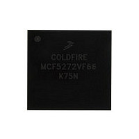
MCF5272VF66 Freescale, MCF5272VF66 Datasheet - Page 330

MCF5272VF66
Manufacturer Part Number
MCF5272VF66
Description
Manufacturer
Freescale
Datasheet
1.MCF5272VF66.pdf
(544 pages)
Specifications of MCF5272VF66
Family Name
MCF5xxx
Device Core
ColdFire
Device Core Size
32b
Frequency (max)
66MHz
Instruction Set Architecture
RISC
Supply Voltage 1 (typ)
3.3V
Operating Temp Range
0C to 70C
Operating Temperature Classification
Commercial
Mounting
Surface Mount
Pin Count
196
Package Type
MA-BGA
Lead Free Status / RoHS Status
Not Compliant
Available stocks
Company
Part Number
Manufacturer
Quantity
Price
Company:
Part Number:
MCF5272VF66
Manufacturer:
HYNIX
Quantity:
19
Company:
Part Number:
MCF5272VF66
Manufacturer:
FREESCAL
Quantity:
885
Company:
Part Number:
MCF5272VF66
Manufacturer:
Freescale Semiconductor
Quantity:
10 000
Part Number:
MCF5272VF66
Manufacturer:
FREESCALE
Quantity:
20 000
Company:
Part Number:
MCF5272VF66J
Manufacturer:
Freescale
Quantity:
256
Company:
Part Number:
MCF5272VF66J
Manufacturer:
Freescale Semiconductor
Quantity:
10 000
Company:
Part Number:
MCF5272VF66R2
Manufacturer:
Freescale Semiconductor
Quantity:
10 000
Company:
Part Number:
MCF5272VF66R2J
Manufacturer:
Freescale Semiconductor
Quantity:
10 000
- Current page: 330 of 544
- Download datasheet (7Mb)
Physical Layer Interface Controller (PLIC)
13.5.22 Clock Select Register (PCSR)
All bits in this register are read/write and are cleared on hardware or software reset.
PCSR controls the PLIC clock generation block. Please refer to
for certain restrictions on the use of the clock generation block.
13-34
14–8
Bits
7–6
5–3
2–0
15
Reset
Field NBP
Addr
R/W
15
CMULT
Name
FDIV
NBP
CKI
—
14
MCF5272 ColdFire
Non-bypass mode select for the clock generation module.
0 The clock generation module is bypassed. Gen_FSC and GDCL are connected to FSC0 and
1 Selects non-bypassed mode. Gen_FSC and GDCL are synthesized from the incoming FSC0
Reserved, should be cleared.
Clock select Input. Selects the source clock for the clock generation block.
00 DCL0
01 FSC0
1x Reserved
FSC divide. Sets the divide ratio between GDCL and Gen_FSC.
000 ÷4
001 ÷8
010 ÷16
011 ÷32
100 ÷64
101 ÷128
110 ÷192
111 ÷256
Clock multiplication ratio. Sets the ratio of the reference clock frequency to the GDCL frequency.
000 x 2
001 x 4
010 x 8
011 x 16
100 x 32
101 x 64
110 x 128
111 x 256
—
DCL0.
or DCL0.
Figure 13-34. Clock Select Register (PCSR)
Table 13-17. PCSR Field Descriptions
8
®
Integrated Microprocessor User’s Manual, Rev. 3
7
CKI
0000_0000_0000_0000
6
MBAR + 0x39E
Read/Write
5
Description
FDIV
Section 13.3, “PLIC Timing
3
2
CMULT
Freescale Semiconductor
Generator,”
0
Related parts for MCF5272VF66
Image
Part Number
Description
Manufacturer
Datasheet
Request
R
Part Number:
Description:
Mcf5272 Coldfire Integrated Microprocessor User
Manufacturer:
Freescale Semiconductor, Inc
Datasheet:

Part Number:
Description:
MCF5272 Interrupt Service Routine for the Physical Layer Interface Controller
Manufacturer:
Freescale Semiconductor / Motorola
Datasheet:

Part Number:
Description:
TOWER ELEVATOR BOARDS HARDWARE
Manufacturer:
Freescale Semiconductor
Datasheet:

Part Number:
Description:
TOWER SERIAL I/O HARDWARE
Manufacturer:
Freescale Semiconductor
Datasheet:

Part Number:
Description:
LCD MODULE FOR TWR SYSTEM
Manufacturer:
Freescale Semiconductor
Datasheet:

Part Number:
Description:
DAUGHTER LCD WVGA I.MX51
Manufacturer:
Freescale Semiconductor
Datasheet:

Part Number:
Description:
TOWER SYSTEM BOARD MPC5125
Manufacturer:
Freescale Semiconductor
Datasheet:

Part Number:
Description:
KIT EVALUATION I.MX51
Manufacturer:
Freescale Semiconductor
Datasheet:

Part Number:
Description:
KIT DEVELOPMENT WINCE IMX25
Manufacturer:
Freescale Semiconductor
Datasheet:

Part Number:
Description:
TOWER SYSTEM KIT MPC5125
Manufacturer:
Freescale Semiconductor
Datasheet:

Part Number:
Description:
TOWER SYSTEM BOARD K40X256
Manufacturer:
Freescale Semiconductor
Datasheet:

Part Number:
Description:
TOWER SYSTEM KIT K40X256
Manufacturer:
Freescale Semiconductor
Datasheet:

Part Number:
Description:
Microcontrollers (MCU) MX28 PLATFORM DEV KIT
Manufacturer:
Freescale Semiconductor
Datasheet:

Part Number:
Description:
MCU, MPU & DSP Development Tools IAR KickStart Kit for Kinetis K60
Manufacturer:
Freescale Semiconductor
Datasheet:

Part Number:
Description:
24BIT HDMI MX535/08
Manufacturer:
Freescale Semiconductor
Datasheet:


