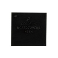
MCF5272VF66 Freescale, MCF5272VF66 Datasheet - Page 309

MCF5272VF66
Manufacturer Part Number
MCF5272VF66
Description
Manufacturer
Freescale
Datasheet
1.MCF5272VF66.pdf
(544 pages)
Specifications of MCF5272VF66
Family Name
MCF5xxx
Device Core
ColdFire
Device Core Size
32b
Frequency (max)
66MHz
Instruction Set Architecture
RISC
Supply Voltage 1 (typ)
3.3V
Operating Temp Range
0C to 70C
Operating Temperature Classification
Commercial
Mounting
Surface Mount
Pin Count
196
Package Type
MA-BGA
Lead Free Status / RoHS Status
Not Compliant
Available stocks
Company
Part Number
Manufacturer
Quantity
Price
Company:
Part Number:
MCF5272VF66
Manufacturer:
HYNIX
Quantity:
19
Company:
Part Number:
MCF5272VF66
Manufacturer:
FREESCAL
Quantity:
885
Company:
Part Number:
MCF5272VF66
Manufacturer:
Freescale Semiconductor
Quantity:
10 000
Part Number:
MCF5272VF66
Manufacturer:
FREESCALE
Quantity:
20 000
Company:
Part Number:
MCF5272VF66J
Manufacturer:
Freescale
Quantity:
256
Company:
Part Number:
MCF5272VF66J
Manufacturer:
Freescale Semiconductor
Quantity:
10 000
Company:
Part Number:
MCF5272VF66R2
Manufacturer:
Freescale Semiconductor
Quantity:
10 000
Company:
Part Number:
MCF5272VF66R2J
Manufacturer:
Freescale Semiconductor
Quantity:
10 000
- Current page: 309 of 544
- Download datasheet (7Mb)
13.3.2
Figure 13-11
possible using P1CR[FSM]. This allows either the port 0 or port 1 timing to be used to generate the 2-KHz
super frame sync interrupt. The SFSC block then divides this accordingly. When P1CR[FSM] is set, FSC1
is the source of the super frame sync. In case P1CR[MS] is 0 (that is, port 1 is in slave mode), the interrupt
is ultimately driven by an external source. In case the M/S bit is 1 (that is, port 1 is in master mode), FSC1
ultimately comes from port 0.
13.3.3
Figure 13-11
through programmable delay 1 referenced to DFSC0. DFSC2 and DFSC3 are generated through
programmable delays 2 and 3 referenced to DFSC1. Note well the following:
13.4
Table 13-1
Freescale Semiconductor
0x030C
0x031C
0x032C
0x033C
0x0300
0x0304
0x0308
0x0310
0x0314
0x0318
0x0320
0x0328
0x0330
0x0334
0x0338
MBAR
Offset
•
•
•
•
P0SDR settings affect DFSC[0–3]
P1SDR settings affect DFSC[1–3]
P2SDR settings affect only DFSC2
P3SDR settings affect only DFSC3
PLIC Register Memory Map
lists the PLIC registers with their offset address from MBAR and their default value on reset.
Super Frame Sync Generation
Frame Sync Synthesis
Port0 D Data Receive
shows the generation of the 2-KHz super frame sync. The choice of either FSC0 or FSC1 is
illustrates the relationships between the various frame sync clocks. DFSC1 is generated
(P0DRR)
[31:24]
MCF5272 ColdFire
Table 13-1. PLIC Module Memory Map
Port1 D Data Receive
®
Integrated Microprocessor User’s Manual, Rev. 3
(P1DRR)
[23:16]
Port0 B1 Data Transmit (P0B1TR)
Port1 B1 Data Transmit (P1B1TR)
Port2 B1 Data Transmit (P2B1TR)
Port3 B1 Data Transmit (P3B1TR)
Port0 B2 Data Transmit (P0B2TR)
Port1 B2 Data Transmit (P1B2TR)
Port0 B1 Data Receive (P0B1RR)
Port1 B1 Data Receive (P1B1RR)
Port2 B1 Data Receive (P2B1RR)
Port3 B1 Data Receive (P3B1RR)
Port0 B2 Data Receive (P0B2RR)
Port1 B2 Data Receive (P1B2RR)
Port2 B2 Data Receive (P2B2RR)
Port3 B2 Data Receive (P3B2RR)
Port2 D Data Receive
(P2DRR)
[15:8]
Physical Layer Interface Controller (PLIC)
Port3 D Data Receive
(P3DRR)
[7:0]
13-13
Related parts for MCF5272VF66
Image
Part Number
Description
Manufacturer
Datasheet
Request
R
Part Number:
Description:
Mcf5272 Coldfire Integrated Microprocessor User
Manufacturer:
Freescale Semiconductor, Inc
Datasheet:

Part Number:
Description:
MCF5272 Interrupt Service Routine for the Physical Layer Interface Controller
Manufacturer:
Freescale Semiconductor / Motorola
Datasheet:

Part Number:
Description:
TOWER ELEVATOR BOARDS HARDWARE
Manufacturer:
Freescale Semiconductor
Datasheet:

Part Number:
Description:
TOWER SERIAL I/O HARDWARE
Manufacturer:
Freescale Semiconductor
Datasheet:

Part Number:
Description:
LCD MODULE FOR TWR SYSTEM
Manufacturer:
Freescale Semiconductor
Datasheet:

Part Number:
Description:
DAUGHTER LCD WVGA I.MX51
Manufacturer:
Freescale Semiconductor
Datasheet:

Part Number:
Description:
TOWER SYSTEM BOARD MPC5125
Manufacturer:
Freescale Semiconductor
Datasheet:

Part Number:
Description:
KIT EVALUATION I.MX51
Manufacturer:
Freescale Semiconductor
Datasheet:

Part Number:
Description:
KIT DEVELOPMENT WINCE IMX25
Manufacturer:
Freescale Semiconductor
Datasheet:

Part Number:
Description:
TOWER SYSTEM KIT MPC5125
Manufacturer:
Freescale Semiconductor
Datasheet:

Part Number:
Description:
TOWER SYSTEM BOARD K40X256
Manufacturer:
Freescale Semiconductor
Datasheet:

Part Number:
Description:
TOWER SYSTEM KIT K40X256
Manufacturer:
Freescale Semiconductor
Datasheet:

Part Number:
Description:
Microcontrollers (MCU) MX28 PLATFORM DEV KIT
Manufacturer:
Freescale Semiconductor
Datasheet:

Part Number:
Description:
MCU, MPU & DSP Development Tools IAR KickStart Kit for Kinetis K60
Manufacturer:
Freescale Semiconductor
Datasheet:

Part Number:
Description:
24BIT HDMI MX535/08
Manufacturer:
Freescale Semiconductor
Datasheet:


