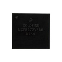
MCF5272VF66 Freescale, MCF5272VF66 Datasheet - Page 509

MCF5272VF66
Manufacturer Part Number
MCF5272VF66
Description
Manufacturer
Freescale
Datasheet
1.MCF5272VF66.pdf
(544 pages)
Specifications of MCF5272VF66
Family Name
MCF5xxx
Device Core
ColdFire
Device Core Size
32b
Frequency (max)
66MHz
Instruction Set Architecture
RISC
Supply Voltage 1 (typ)
3.3V
Operating Temp Range
0C to 70C
Operating Temperature Classification
Commercial
Mounting
Surface Mount
Pin Count
196
Package Type
MA-BGA
Lead Free Status / RoHS Status
Not Compliant
Available stocks
Company
Part Number
Manufacturer
Quantity
Price
Company:
Part Number:
MCF5272VF66
Manufacturer:
HYNIX
Quantity:
19
Company:
Part Number:
MCF5272VF66
Manufacturer:
FREESCAL
Quantity:
885
Company:
Part Number:
MCF5272VF66
Manufacturer:
Freescale Semiconductor
Quantity:
10 000
Part Number:
MCF5272VF66
Manufacturer:
FREESCALE
Quantity:
20 000
Company:
Part Number:
MCF5272VF66J
Manufacturer:
Freescale
Quantity:
256
Company:
Part Number:
MCF5272VF66J
Manufacturer:
Freescale Semiconductor
Quantity:
10 000
Company:
Part Number:
MCF5272VF66R2
Manufacturer:
Freescale Semiconductor
Quantity:
10 000
Company:
Part Number:
MCF5272VF66R2J
Manufacturer:
Freescale Semiconductor
Quantity:
10 000
- Current page: 509 of 544
- Download datasheet (7Mb)
Figure 23-18
Table 23-19
Freescale Semiconductor
Name
P30
P31
P32
P33
P34
P35
P38
P39
P40
P41
P42
FSC input high before the falling edge of DCL0, DCL1 (setup time)
FSC0 input low before the rising edge of DCL0 (deassertion setup time),
FSC1 input low before the rising edge of DCL1 (deassertion setup time)
FSC0 input high after the falling edge of DCL0 (hold time),
FSC1 input high after the falling edge of DCL1 (hold time)
DCL0, DCL1 clock frequency
DCL0, DCL1 pulse-width low
DCL0, DCL1 pulse-width high
Delay from rising edge of FSC0 to low-z and valid data on DOUT0
Delay from rising edge of FSC1 to low-z and valid data on DOUT1
Delay from rising edge of DFSC2 to low-z and valid data on DOUT1
Delay from rising edge of DFSC3 to low-z and valid data on DOUT1, DOUT3
Delay from rising edge of DCL0 to data valid on DOUT0,
Delay from rising edge of DCL1 to data valid on DOUT1, DOUT3
Delay from rising edge of DCL0 to high-z on DOUT0,
Delay from rising edge of DCL1 to high-Z on DOUT1, DOUT3
Data valid on DIN0 before rising edge of DCL0,
Data valid on DIN1 or DIN3 before rising edge of DCL1
Data valid on DIN0 after rising edge of DCL0,
Data valid on DIN1 or DIN3 after rising edge of DCL1
DOUT[0,1,3]
DFSC[2:3]
FSR[0,1]
DCL[0:1]
DIN[0:3]
lists timings for GCI slave mode.
shows IDL slave timings listed in
P15
MCF5272 ColdFire
Table 23-19. GCI Slave Mode Timing, PLIC Ports 0–3
P16
P17
P20
Characteristic
Figure 23-18. IDL Slave Timing
®
Integrated Microprocessor User’s Manual, Rev. 3
P25
P21
Table
P26
23-18.
P14
P18
P23
P14
P19
P24
P22
Min
25
25
25
45
45
25
25
—
—
—
—
8192
Max
55
55
30
30
30
—
—
—
—
Electrical Characteristics
% of DCL period
% of DCL period
Unit
KHz
nS
nS
nS
nS
nS
nS
nS
nS
23-25
Related parts for MCF5272VF66
Image
Part Number
Description
Manufacturer
Datasheet
Request
R
Part Number:
Description:
Mcf5272 Coldfire Integrated Microprocessor User
Manufacturer:
Freescale Semiconductor, Inc
Datasheet:

Part Number:
Description:
MCF5272 Interrupt Service Routine for the Physical Layer Interface Controller
Manufacturer:
Freescale Semiconductor / Motorola
Datasheet:

Part Number:
Description:
TOWER ELEVATOR BOARDS HARDWARE
Manufacturer:
Freescale Semiconductor
Datasheet:

Part Number:
Description:
TOWER SERIAL I/O HARDWARE
Manufacturer:
Freescale Semiconductor
Datasheet:

Part Number:
Description:
LCD MODULE FOR TWR SYSTEM
Manufacturer:
Freescale Semiconductor
Datasheet:

Part Number:
Description:
DAUGHTER LCD WVGA I.MX51
Manufacturer:
Freescale Semiconductor
Datasheet:

Part Number:
Description:
TOWER SYSTEM BOARD MPC5125
Manufacturer:
Freescale Semiconductor
Datasheet:

Part Number:
Description:
KIT EVALUATION I.MX51
Manufacturer:
Freescale Semiconductor
Datasheet:

Part Number:
Description:
KIT DEVELOPMENT WINCE IMX25
Manufacturer:
Freescale Semiconductor
Datasheet:

Part Number:
Description:
TOWER SYSTEM KIT MPC5125
Manufacturer:
Freescale Semiconductor
Datasheet:

Part Number:
Description:
TOWER SYSTEM BOARD K40X256
Manufacturer:
Freescale Semiconductor
Datasheet:

Part Number:
Description:
TOWER SYSTEM KIT K40X256
Manufacturer:
Freescale Semiconductor
Datasheet:

Part Number:
Description:
Microcontrollers (MCU) MX28 PLATFORM DEV KIT
Manufacturer:
Freescale Semiconductor
Datasheet:

Part Number:
Description:
MCU, MPU & DSP Development Tools IAR KickStart Kit for Kinetis K60
Manufacturer:
Freescale Semiconductor
Datasheet:

Part Number:
Description:
24BIT HDMI MX535/08
Manufacturer:
Freescale Semiconductor
Datasheet:


