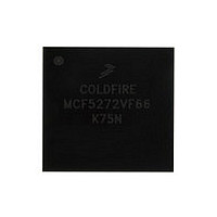
MCF5272VF66 Freescale, MCF5272VF66 Datasheet - Page 275

MCF5272VF66
Manufacturer Part Number
MCF5272VF66
Description
Manufacturer
Freescale
Datasheet
1.MCF5272VF66.pdf
(544 pages)
Specifications of MCF5272VF66
Family Name
MCF5xxx
Device Core
ColdFire
Device Core Size
32b
Frequency (max)
66MHz
Instruction Set Architecture
RISC
Supply Voltage 1 (typ)
3.3V
Operating Temp Range
0C to 70C
Operating Temperature Classification
Commercial
Mounting
Surface Mount
Pin Count
196
Package Type
MA-BGA
Lead Free Status / RoHS Status
Not Compliant
Available stocks
Company
Part Number
Manufacturer
Quantity
Price
Company:
Part Number:
MCF5272VF66
Manufacturer:
HYNIX
Quantity:
19
Company:
Part Number:
MCF5272VF66
Manufacturer:
FREESCAL
Quantity:
885
Company:
Part Number:
MCF5272VF66
Manufacturer:
Freescale Semiconductor
Quantity:
10 000
Part Number:
MCF5272VF66
Manufacturer:
FREESCALE
Quantity:
20 000
Company:
Part Number:
MCF5272VF66J
Manufacturer:
Freescale
Quantity:
256
Company:
Part Number:
MCF5272VF66J
Manufacturer:
Freescale Semiconductor
Quantity:
10 000
Company:
Part Number:
MCF5272VF66R2
Manufacturer:
Freescale Semiconductor
Quantity:
10 000
Company:
Part Number:
MCF5272VF66R2J
Manufacturer:
Freescale Semiconductor
Quantity:
10 000
- Current page: 275 of 544
- Download datasheet (7Mb)
12.3.2.13 USB Endpoint 0 Control Register (EP0CTL)
Figure 12-16
specific control (bits 0-9) functions.
Table 12-12
Freescale Semiconductor
31–19
Bits
18
17
16
15
Reset
Reset
Reset
Reset
Field
Field
Field
Field
Addr
R/W
R/W
R/W
R/W
WOR_LVL
WOR_EN
CLK_SEL
DEBUG
lists field descriptions for the USB endpoint 0 control register.
Name
shows the USB endpoint 0 control register. provides both module level and endpoint 0
CRC_ERR
CLK_SEL
—
31
22
15
7
MCF5272 ColdFire
Figure 12-16. USB Endpoint 0 Control Register (EP0CTL)
Reserved, should be cleared.
Debug mode. Enters debug mode. Debug mode enables CRC error generation and notification of
a change of address.
0 Normal operation
1 Enable debug mode functions
Wake-on-ring level select. Selects the active level of INT1 for the wake-on-ring function.
0 Wake-on-ring function is invoked when INT1 pin is 0.
1 Wake-on-ring function is invoked when INT1 pin is 1.
Wake-on-ring enable. Generates a RESUME when the active level is detected on INT1 pin.
0 Wake-on-ring function disabled
1 Wake-on-ring function enabled
Note: the wake-on-ring function generates a RESUME only if the USB module is enabled for
remote wakeup by the host, for example, WAKE_ST = 1, and is suspended.
Clock source selection. Overrides the clock source for the USB module. If the USB_ExtCLK pin is
selected after reset, setting this bit forces the USB module to use the internal system clock.
0 Clock is retrieved from the clock selected at reset.
1 Clock is retrieved from the internal system clock.
Note: the selected clock must have a frequency of 48 MHz.
RESUME
—
14
6
Table 12-12. EP0CTL Field Descriptions
AFE_EN
—
®
13
5
Integrated Microprocessor User’s Manual, Rev. 3
OUT_LVL
BUS_PWR USB_EN CFG_RAM_VAL CMD_ERR CMD_OVER
MBAR + 0x104C
12
4
0000_0000
0000_0000
0000_0000
0000_0000
R/W
R/W
R/W
R/W
—
19
11
3
Description
IN_LVL
DEBUG
18
10
2
WOR_LVL
IN_DONE
17
9
1
Universal Serial Bus (USB)
WOR_EN
—
23
16
8
0
12-17
Related parts for MCF5272VF66
Image
Part Number
Description
Manufacturer
Datasheet
Request
R
Part Number:
Description:
Mcf5272 Coldfire Integrated Microprocessor User
Manufacturer:
Freescale Semiconductor, Inc
Datasheet:

Part Number:
Description:
MCF5272 Interrupt Service Routine for the Physical Layer Interface Controller
Manufacturer:
Freescale Semiconductor / Motorola
Datasheet:

Part Number:
Description:
TOWER ELEVATOR BOARDS HARDWARE
Manufacturer:
Freescale Semiconductor
Datasheet:

Part Number:
Description:
TOWER SERIAL I/O HARDWARE
Manufacturer:
Freescale Semiconductor
Datasheet:

Part Number:
Description:
LCD MODULE FOR TWR SYSTEM
Manufacturer:
Freescale Semiconductor
Datasheet:

Part Number:
Description:
DAUGHTER LCD WVGA I.MX51
Manufacturer:
Freescale Semiconductor
Datasheet:

Part Number:
Description:
TOWER SYSTEM BOARD MPC5125
Manufacturer:
Freescale Semiconductor
Datasheet:

Part Number:
Description:
KIT EVALUATION I.MX51
Manufacturer:
Freescale Semiconductor
Datasheet:

Part Number:
Description:
KIT DEVELOPMENT WINCE IMX25
Manufacturer:
Freescale Semiconductor
Datasheet:

Part Number:
Description:
TOWER SYSTEM KIT MPC5125
Manufacturer:
Freescale Semiconductor
Datasheet:

Part Number:
Description:
TOWER SYSTEM BOARD K40X256
Manufacturer:
Freescale Semiconductor
Datasheet:

Part Number:
Description:
TOWER SYSTEM KIT K40X256
Manufacturer:
Freescale Semiconductor
Datasheet:

Part Number:
Description:
Microcontrollers (MCU) MX28 PLATFORM DEV KIT
Manufacturer:
Freescale Semiconductor
Datasheet:

Part Number:
Description:
MCU, MPU & DSP Development Tools IAR KickStart Kit for Kinetis K60
Manufacturer:
Freescale Semiconductor
Datasheet:

Part Number:
Description:
24BIT HDMI MX535/08
Manufacturer:
Freescale Semiconductor
Datasheet:


