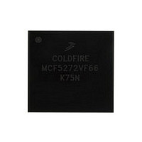
MCF5272VF66 Freescale, MCF5272VF66 Datasheet - Page 354

MCF5272VF66
Manufacturer Part Number
MCF5272VF66
Description
Manufacturer
Freescale
Datasheet
1.MCF5272VF66.pdf
(544 pages)
Specifications of MCF5272VF66
Family Name
MCF5xxx
Device Core
ColdFire
Device Core Size
32b
Frequency (max)
66MHz
Instruction Set Architecture
RISC
Supply Voltage 1 (typ)
3.3V
Operating Temp Range
0C to 70C
Operating Temperature Classification
Commercial
Mounting
Surface Mount
Pin Count
196
Package Type
MA-BGA
Lead Free Status / RoHS Status
Not Compliant
Available stocks
Company
Part Number
Manufacturer
Quantity
Price
Company:
Part Number:
MCF5272VF66
Manufacturer:
HYNIX
Quantity:
19
Company:
Part Number:
MCF5272VF66
Manufacturer:
FREESCAL
Quantity:
885
Company:
Part Number:
MCF5272VF66
Manufacturer:
Freescale Semiconductor
Quantity:
10 000
Part Number:
MCF5272VF66
Manufacturer:
FREESCALE
Quantity:
20 000
Company:
Part Number:
MCF5272VF66J
Manufacturer:
Freescale
Quantity:
256
Company:
Part Number:
MCF5272VF66J
Manufacturer:
Freescale Semiconductor
Quantity:
10 000
Company:
Part Number:
MCF5272VF66R2
Manufacturer:
Freescale Semiconductor
Quantity:
10 000
Company:
Part Number:
MCF5272VF66R2J
Manufacturer:
Freescale Semiconductor
Quantity:
10 000
- Current page: 354 of 544
- Download datasheet (7Mb)
Queued Serial Peripheral Interface (QSPI) Module
14.5.8
The following steps are necessary to set up the QSPI 12-bit data transfers and a QSPI_CLK of 4.125 MHz.
The QSPI RAM is set up for a queue of 16 transfers. All four QSPI_CS signals are used in this example.
14-16
1. Enable all QSPI_CS pins on the MCF5272. Write PACNT with 0x0080_4000 to enable QSPI_CS1
2. Write the QMR with 0xB308 to set up 12-bit data words with the data shifted on the falling clock
3. Write QDLYR with the desired delays.
4. Write QIR with 0xD00D to enable write collision, abort bus errors, and clear any interrupts.
5. Write QAR with 0x0020 to select the first command RAM entry.
6. Write QDR with 0x7E00, 0x7E00, 0x7E00, 0x7E00, 0x7D00, 0x7D00, 0x7D00, 0x7D00, 0x7B00,
7. Write QAR with 0x0000 to select the first transmit RAM entry.
8. Write QDR with sixteen 12-bit words of data.
9. Write QWR with 0x0F00 to set up a queue beginning at entry 0 and ending at entry 15.
10. Set QDLYR[SPE] to enable the transfers.
11. Wait until the transfers are complete. QIR[SPIF] is set when the transfers are complete.
12. Write QAR with 0x0010 to select the first receive RAM entry.
13. Read QDR to get the received data for each transfer.
14. Repeat steps 5 through 13 to do another transfer.
and QSPI_CS3.Write PDCNT with 0x0000_0030 to enable QSPI_CS2.
edge, and a clock frequency of 4.125 MHz (assuming a 66-MHz CLKIN).
0x7B00, 0x7B00, 0x7B00, 0x7700, 0x7700, 0x7700, and 0x7700 to set up four transfers for each
chip select. The chip selects are active low in this example.
Programming Example
MCF5272 ColdFire
®
Integrated Microprocessor User’s Manual, Rev. 3
Freescale Semiconductor
Related parts for MCF5272VF66
Image
Part Number
Description
Manufacturer
Datasheet
Request
R
Part Number:
Description:
Mcf5272 Coldfire Integrated Microprocessor User
Manufacturer:
Freescale Semiconductor, Inc
Datasheet:

Part Number:
Description:
MCF5272 Interrupt Service Routine for the Physical Layer Interface Controller
Manufacturer:
Freescale Semiconductor / Motorola
Datasheet:

Part Number:
Description:
TOWER ELEVATOR BOARDS HARDWARE
Manufacturer:
Freescale Semiconductor
Datasheet:

Part Number:
Description:
TOWER SERIAL I/O HARDWARE
Manufacturer:
Freescale Semiconductor
Datasheet:

Part Number:
Description:
LCD MODULE FOR TWR SYSTEM
Manufacturer:
Freescale Semiconductor
Datasheet:

Part Number:
Description:
DAUGHTER LCD WVGA I.MX51
Manufacturer:
Freescale Semiconductor
Datasheet:

Part Number:
Description:
TOWER SYSTEM BOARD MPC5125
Manufacturer:
Freescale Semiconductor
Datasheet:

Part Number:
Description:
KIT EVALUATION I.MX51
Manufacturer:
Freescale Semiconductor
Datasheet:

Part Number:
Description:
KIT DEVELOPMENT WINCE IMX25
Manufacturer:
Freescale Semiconductor
Datasheet:

Part Number:
Description:
TOWER SYSTEM KIT MPC5125
Manufacturer:
Freescale Semiconductor
Datasheet:

Part Number:
Description:
TOWER SYSTEM BOARD K40X256
Manufacturer:
Freescale Semiconductor
Datasheet:

Part Number:
Description:
TOWER SYSTEM KIT K40X256
Manufacturer:
Freescale Semiconductor
Datasheet:

Part Number:
Description:
Microcontrollers (MCU) MX28 PLATFORM DEV KIT
Manufacturer:
Freescale Semiconductor
Datasheet:

Part Number:
Description:
MCU, MPU & DSP Development Tools IAR KickStart Kit for Kinetis K60
Manufacturer:
Freescale Semiconductor
Datasheet:

Part Number:
Description:
24BIT HDMI MX535/08
Manufacturer:
Freescale Semiconductor
Datasheet:


