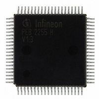
PEB2255H-V13 Infineon Technologies, PEB2255H-V13 Datasheet - Page 285

PEB2255H-V13
Manufacturer Part Number
PEB2255H-V13
Description
IC INTERFACE LINE 80-MQFP
Manufacturer
Infineon Technologies
Datasheet
1.PEB2255H-V13.pdf
(374 pages)
Specifications of PEB2255H-V13
Applications
*
Interface
*
Voltage - Supply
*
Package / Case
80-SQFP
Mounting Type
Surface Mount
Lead Free Status / RoHS Status
Lead free / RoHS Compliant
Other names
PEB2255H-V13
PEB2255H-V13IN
PEB2255H-V13IN
Available stocks
Company
Part Number
Manufacturer
Quantity
Price
Company:
Part Number:
PEB2255H-V13
Manufacturer:
Infineon Technologies
Quantity:
10 000
- Current page: 285 of 374
- Download datasheet (6Mb)
SICS…
CRCI…
XCRCI…
RDIS…
RCO2…RCO0… Receive Offset/Receive Frame Marker Offset
Data Sheet
System Interface Channel Select
0
Data in the second channel phase is tristated.
Data on pin XDI is sampled in the first channel phase only. Data in the
second channel phase is ignored.
1
phase. Data in the first channel phase is tristated.
Data on pin XDI is sampled in the second channel phase only. Data
in the first channel phase is ignored.
Automatic CRC6 Bit Inversion
If set, all CRC bits of one outgoing extended multiframe are inverted
in case a CRC error is flagged for the previous received multiframe.
This function is logically ORed with RC0.XCRCI.
Transmit CRC6 Bit Inversion
If set, the CRC bits in the outgoing data stream are inverted before
transmission. This function is logically ORed with RC0.CRCI.
Receive Data Input Sense
Only applicable for dual rail mode (LIM1.DRS = 1).
0
1
Depending on bit SIC2.SRFSO this bit enables different functions:
Receive Clock-Slot Offset (SIC2.SRFSO = 0)
Initial value loaded into the receive bit counter at the trigger edge of
SCLKR when the synchronous pulse on port SYPR is active. Setting
of SIC1.SRSC enforces programming the offset values in a range of
0 to 192 bits with RCO0 always cleared.
Receive Frame Marker Offset (SIC2.SRFSO = 1)
Offset programming of the receive frame marker which is output on
port SYPR. The receive frame marker could be activated during any
bit position of the current frame.
Calculation of the value X of the “Receive Counter Offset” register
RC1/0 depends on the bit position BP which should be marked and
SCLKR: X = (2BP) mod 386, for SCLKR = 1.544 MHz
Applicable only if bit FMR1.IMOD (4-MHz system interface) is
cleared.
Received data is output on port RDO in the first channel phase.
Inputs: RDIP, RDIN active low, input ROID is active high
Inputs: RDIP, RDIN active high, input ROID is active low
Received data is output on port RDO in the second channel
285
FALC-LH V1.3
T1/J1 Registers
PEB 2255
2000-07
Related parts for PEB2255H-V13
Image
Part Number
Description
Manufacturer
Datasheet
Request
R

Part Number:
Description:
E1/t1/j1 Framer And Line Interface Component For Long And Short Haul Applications
Manufacturer:
Infineon Technologies Corporation
Datasheet:

Part Number:
Description:
Manufacturer:
Infineon Technologies AG
Datasheet:

Part Number:
Description:
Manufacturer:
Infineon Technologies AG
Datasheet:

Part Number:
Description:
Manufacturer:
Infineon Technologies AG
Datasheet:

Part Number:
Description:
Manufacturer:
Infineon Technologies AG
Datasheet:

Part Number:
Description:
Manufacturer:
Infineon Technologies AG
Datasheet:

Part Number:
Description:
Manufacturer:
Infineon Technologies AG
Datasheet:

Part Number:
Description:
Manufacturer:
Infineon Technologies AG
Datasheet:

Part Number:
Description:
16-bit microcontroller with 2x2 KByte RAM
Manufacturer:
Infineon Technologies AG
Datasheet:

Part Number:
Description:
NPN silicon RF transistor
Manufacturer:
Infineon Technologies AG
Datasheet:

Part Number:
Description:
NPN silicon RF transistor
Manufacturer:
Infineon Technologies AG
Datasheet:

Part Number:
Description:
NPN silicon RF transistor
Manufacturer:
Infineon Technologies AG
Datasheet:

Part Number:
Description:
NPN silicon RF transistor
Manufacturer:
Infineon Technologies AG
Datasheet:

Part Number:
Description:
Si-MMIC-amplifier in SIEGET 25-technologie
Manufacturer:
Infineon Technologies AG
Datasheet:

Part Number:
Description:
IGBT Power Module
Manufacturer:
Infineon Technologies AG
Datasheet:


