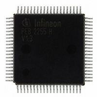
PEB2255H-V13 Infineon Technologies, PEB2255H-V13 Datasheet - Page 58

PEB2255H-V13
Manufacturer Part Number
PEB2255H-V13
Description
IC INTERFACE LINE 80-MQFP
Manufacturer
Infineon Technologies
Datasheet
1.PEB2255H-V13.pdf
(374 pages)
Specifications of PEB2255H-V13
Applications
*
Interface
*
Voltage - Supply
*
Package / Case
80-SQFP
Mounting Type
Surface Mount
Lead Free Status / RoHS Status
Lead free / RoHS Compliant
Other names
PEB2255H-V13
PEB2255H-V13IN
PEB2255H-V13IN
Available stocks
Company
Part Number
Manufacturer
Quantity
Price
Company:
Part Number:
PEB2255H-V13
Manufacturer:
Infineon Technologies
Quantity:
10 000
- Current page: 58 of 374
- Download datasheet (6Mb)
4.1.6
The receive jitter attenuator is placed in the receive path. The jitter attenuator meets the
requirements of ITU-T I.431, G. 736-739, G.823 and ETSI TBR12/13.
The internal DCO-R generates a “jitter free“ output clock which is directly dependent on
the phase difference of the incoming clock and the jitter attenuated clock.The receive
jitter attenuator can be either synchronized with the extracted receive clock RCLK or to
a 2.048-MHz clock provided on pin SYNC. The received data is written into the receive
elastic buffer with RCLK and are read out with the dejittered clock CLK8M/CLKX sourced
by DCO-R if it is connected to SCLKR. Optionally a 8 kHz clock is provided on pin XCLK/
FSC or FSC.
The DCO-R circuitry attenuates the incoming jittered clock starting at 2 Hz jitter
frequency with 20 dB per decade fall off. Wander with a jitter frequency below 2 Hz is
passed unattenuated. The intrinsic jitter in the absence of any input jitter is < 0.02 UI.
For some applications it might be useful starting of jitter attenuation at lower frequencies.
Therefore the corner frequency is switchable by the factor of ten down to 0.2 Hz
(LIM2.SCF).
Jitter attenuation can be achieved either using an external tunable crystal on pins
XTAL1/XTAL2 or using the crystal-less jitter attenuation selected by LIM2.DJA1/2. In this
case, a stable clock or regular crystal of 16.384 MHz has to be provided on pin XTAL1
(+/- 50 ppm). In crystal-less mode the system clock output on pin CLK16M can be either
the dejittered or the non-dejittered clock (LIM3.CSC).
The DCO-R circuitry is automatically centered to the nominal bit rate if the reference
clock on pin SYNC/RCLK is missed for two 2.048-MHz clock periods. In analog line
interface mode the RCLK is always running. Only in digital line interface mode with single
rail data a gapped clock at RCLKI may occur. In this case, DCO-R centers automatically.
The receive jitter attenuator works in two different modes:
• Slave mode
• Master mode
The following table shows the clock modes with the corresponding synchronization
sources.
Data Sheet
In Slave mode (LIM0.MAS = 0) the DCO-R is synchronized with the recovered route
clock. In case of LOS the DCO-R switches to Master mode automatically.
In Master mode (LIM0.MAS = 1) the jitter attenuator is in free running mode if no clock
on pin SYNC is supplied. If a 2.048 MHz clock at the SYNC input is applied the DCO-
R synchronizes to this input.
Receive Jitter Attenuator (E1)
58
Functional Description E1
FALC-LH V1.3
PEB 2255
2000-07
Related parts for PEB2255H-V13
Image
Part Number
Description
Manufacturer
Datasheet
Request
R

Part Number:
Description:
E1/t1/j1 Framer And Line Interface Component For Long And Short Haul Applications
Manufacturer:
Infineon Technologies Corporation
Datasheet:

Part Number:
Description:
Manufacturer:
Infineon Technologies AG
Datasheet:

Part Number:
Description:
Manufacturer:
Infineon Technologies AG
Datasheet:

Part Number:
Description:
Manufacturer:
Infineon Technologies AG
Datasheet:

Part Number:
Description:
Manufacturer:
Infineon Technologies AG
Datasheet:

Part Number:
Description:
Manufacturer:
Infineon Technologies AG
Datasheet:

Part Number:
Description:
Manufacturer:
Infineon Technologies AG
Datasheet:

Part Number:
Description:
Manufacturer:
Infineon Technologies AG
Datasheet:

Part Number:
Description:
16-bit microcontroller with 2x2 KByte RAM
Manufacturer:
Infineon Technologies AG
Datasheet:

Part Number:
Description:
NPN silicon RF transistor
Manufacturer:
Infineon Technologies AG
Datasheet:

Part Number:
Description:
NPN silicon RF transistor
Manufacturer:
Infineon Technologies AG
Datasheet:

Part Number:
Description:
NPN silicon RF transistor
Manufacturer:
Infineon Technologies AG
Datasheet:

Part Number:
Description:
NPN silicon RF transistor
Manufacturer:
Infineon Technologies AG
Datasheet:

Part Number:
Description:
Si-MMIC-amplifier in SIEGET 25-technologie
Manufacturer:
Infineon Technologies AG
Datasheet:

Part Number:
Description:
IGBT Power Module
Manufacturer:
Infineon Technologies AG
Datasheet:


