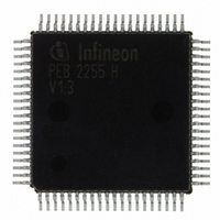
PEB2255H-V13 Infineon Technologies, PEB2255H-V13 Datasheet - Page 69

PEB2255H-V13
Manufacturer Part Number
PEB2255H-V13
Description
IC INTERFACE LINE 80-MQFP
Manufacturer
Infineon Technologies
Datasheet
1.PEB2255H-V13.pdf
(374 pages)
Specifications of PEB2255H-V13
Applications
*
Interface
*
Voltage - Supply
*
Package / Case
80-SQFP
Mounting Type
Surface Mount
Lead Free Status / RoHS Status
Lead free / RoHS Compliant
Other names
PEB2255H-V13
PEB2255H-V13IN
PEB2255H-V13IN
Available stocks
Company
Part Number
Manufacturer
Quantity
Price
Company:
Part Number:
PEB2255H-V13
Manufacturer:
Infineon Technologies
Quantity:
10 000
- Current page: 69 of 374
- Download datasheet (6Mb)
4.2
The FALC
receive direction different system clocks and system pulses are necessary. The interface
to the receive system highway is realized by two data buses, one for the data RDO and
one for the signaling data RSIG. The receive highway is clocked via pin SCLKR/RCLK,
while the interface to the transmit system highway is independently clocked via pin
SCLKX. Selectable system clock and data rates and their valid combinations are shown
in the table below.
Table 13
System Data Rate
2.048 Mbit/s
4.096 Mbit/s
1)
Generally the data or marker on the system interface are clocked off or latched on the
falling edge of the SCLKR/X clock. 8.192-MHz clocking rate allows transmitting of time
slots in different channel phases. The active channel phase is selected by RC0.SICS,
during the inactive channel phase the output signal is tristated. The signals on pin SYPR
in conjunction with the assigned timeslot offset in register RC0 and RC1 define the
beginning of a frame on the receive system highway. The signal on pin SYPX in
conjunction with the assigned timeslot offset in register XC0 and XC1 define the
beginning of a frame on the transmit system highway.
Adjusting the frame begin (time slot 0, bit 0) relative to SYPR/X can be programmed in
clock steps in the range of 0...125 µsec.
A receive frame marker RFM can be activated during any bit position of the entire frame.
Programming is done with registers RC1/0. The pin function RFM is selected by
SIC2.SRFS0. The receive frame marker is active high for one 2.048 MHz cycle
(2.048 Mbit/s PCM highway interface mode) or two 8.192 MHz cycles (4.096 Mbit/s PCM
highway interface mode) and is clocked off with the falling edge of the clock which is in/
output on port SCLKR.
Data Sheet
x = valid; -- = invalid
®
System Interface in E1 Mode
-LH offers a flexible feature for system designers where for transmit and
System Clock and Data Rates (E1)
Clock Rate 2.048 MHz
x
69
--
1)
Functional Description E1
Clock Rate 8.192 MHz
FALC-LH V1.3
x
x
PEB 2255
2000-07
Related parts for PEB2255H-V13
Image
Part Number
Description
Manufacturer
Datasheet
Request
R

Part Number:
Description:
E1/t1/j1 Framer And Line Interface Component For Long And Short Haul Applications
Manufacturer:
Infineon Technologies Corporation
Datasheet:

Part Number:
Description:
Manufacturer:
Infineon Technologies AG
Datasheet:

Part Number:
Description:
Manufacturer:
Infineon Technologies AG
Datasheet:

Part Number:
Description:
Manufacturer:
Infineon Technologies AG
Datasheet:

Part Number:
Description:
Manufacturer:
Infineon Technologies AG
Datasheet:

Part Number:
Description:
Manufacturer:
Infineon Technologies AG
Datasheet:

Part Number:
Description:
Manufacturer:
Infineon Technologies AG
Datasheet:

Part Number:
Description:
Manufacturer:
Infineon Technologies AG
Datasheet:

Part Number:
Description:
16-bit microcontroller with 2x2 KByte RAM
Manufacturer:
Infineon Technologies AG
Datasheet:

Part Number:
Description:
NPN silicon RF transistor
Manufacturer:
Infineon Technologies AG
Datasheet:

Part Number:
Description:
NPN silicon RF transistor
Manufacturer:
Infineon Technologies AG
Datasheet:

Part Number:
Description:
NPN silicon RF transistor
Manufacturer:
Infineon Technologies AG
Datasheet:

Part Number:
Description:
NPN silicon RF transistor
Manufacturer:
Infineon Technologies AG
Datasheet:

Part Number:
Description:
Si-MMIC-amplifier in SIEGET 25-technologie
Manufacturer:
Infineon Technologies AG
Datasheet:

Part Number:
Description:
IGBT Power Module
Manufacturer:
Infineon Technologies AG
Datasheet:


