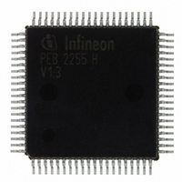
PEB2255H-V13 Infineon Technologies, PEB2255H-V13 Datasheet - Page 35

PEB2255H-V13
Manufacturer Part Number
PEB2255H-V13
Description
IC INTERFACE LINE 80-MQFP
Manufacturer
Infineon Technologies
Datasheet
1.PEB2255H-V13.pdf
(374 pages)
Specifications of PEB2255H-V13
Applications
*
Interface
*
Voltage - Supply
*
Package / Case
80-SQFP
Mounting Type
Surface Mount
Lead Free Status / RoHS Status
Lead free / RoHS Compliant
Other names
PEB2255H-V13
PEB2255H-V13IN
PEB2255H-V13IN
Available stocks
Company
Part Number
Manufacturer
Quantity
Price
Company:
Part Number:
PEB2255H-V13
Manufacturer:
Infineon Technologies
Quantity:
10 000
- Current page: 35 of 374
- Download datasheet (6Mb)
•
Table 4
Pin No.
57
70
Data Sheet
RDO
DLR
Symbol
RSIG
Pin Definitions - System Interface
Input (I)
Output (O)
Supply (S)
O
O
O
System Interface Receive
Function
Receive Data Out
Received data which is sent to the system
highway at 4096 kbit/s, 2048 kbit/s or
1544 kbit/s (T1/J1 only). In 4096 kbit/s mode
data is shifted out in the channel phase which is
selected by RC0.SICS. During the other channel
phase RDO is set into tristate.
Clocking off data is done with the falling edge of
SCLKR or RCLK, if the receive elastic store is
bypassed. The delay between the beginning of
time-slot 0 and the initial edge of SCLKR (after
SYPR goes active) is determined by the values
of registers RC1 and RC0.
Data Link Bit Receive
E1 mode:
Marks the S
RDO. The S
every frame not containing the frame alignment
signal are selected by register XC0.SA4E-
SA8E.
T1/J1 mode:
Provides a signal which marks the DL bit
position within the data stream on RDO. It can
be used as receive strobe signal for external
data link controllers. In 4096 kbit/s mode DLR is
active only during the channel phase selected by
RCO.SICS.
Receive Signaling Data
Output for receive signaling data sent to the
signaling highway.
This function is selected by setting
LOOP.SPN = 1
LIM3.ESY = 1
XSP.CASEN = 0
35
A
A
4...8 bits within the data steam on
4...8 bit positions in time slot 0 of
Pin Descriptions
FALC-LH V1.3
PEB 2255
2000-07
Related parts for PEB2255H-V13
Image
Part Number
Description
Manufacturer
Datasheet
Request
R

Part Number:
Description:
E1/t1/j1 Framer And Line Interface Component For Long And Short Haul Applications
Manufacturer:
Infineon Technologies Corporation
Datasheet:

Part Number:
Description:
Manufacturer:
Infineon Technologies AG
Datasheet:

Part Number:
Description:
Manufacturer:
Infineon Technologies AG
Datasheet:

Part Number:
Description:
Manufacturer:
Infineon Technologies AG
Datasheet:

Part Number:
Description:
Manufacturer:
Infineon Technologies AG
Datasheet:

Part Number:
Description:
Manufacturer:
Infineon Technologies AG
Datasheet:

Part Number:
Description:
Manufacturer:
Infineon Technologies AG
Datasheet:

Part Number:
Description:
Manufacturer:
Infineon Technologies AG
Datasheet:

Part Number:
Description:
16-bit microcontroller with 2x2 KByte RAM
Manufacturer:
Infineon Technologies AG
Datasheet:

Part Number:
Description:
NPN silicon RF transistor
Manufacturer:
Infineon Technologies AG
Datasheet:

Part Number:
Description:
NPN silicon RF transistor
Manufacturer:
Infineon Technologies AG
Datasheet:

Part Number:
Description:
NPN silicon RF transistor
Manufacturer:
Infineon Technologies AG
Datasheet:

Part Number:
Description:
NPN silicon RF transistor
Manufacturer:
Infineon Technologies AG
Datasheet:

Part Number:
Description:
Si-MMIC-amplifier in SIEGET 25-technologie
Manufacturer:
Infineon Technologies AG
Datasheet:

Part Number:
Description:
IGBT Power Module
Manufacturer:
Infineon Technologies AG
Datasheet:


