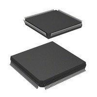
D12332VFC25 Renesas Electronics America, D12332VFC25 Datasheet - Page 1133

D12332VFC25
Manufacturer Part Number
D12332VFC25
Description
MCU 3V 0K 144-QFP
Manufacturer
Renesas Electronics America
Series
H8® H8S/2300r
Datasheet
1.DF2338VFC25V.pdf
(1246 pages)
Specifications of D12332VFC25
Core Processor
H8S/2000
Core Size
16-Bit
Speed
25MHz
Connectivity
SCI, SmartCard
Peripherals
DMA, POR, PWM, WDT
Number Of I /o
106
Program Memory Type
ROMless
Ram Size
8K x 8
Voltage - Supply (vcc/vdd)
2.7 V ~ 3.6 V
Data Converters
A/D 12x10b; D/A 4x8b
Oscillator Type
Internal
Operating Temperature
-20°C ~ 75°C
Package / Case
144-QFP
Lead Free Status / RoHS Status
Contains lead / RoHS non-compliant
Eeprom Size
-
Program Memory Size
-
Other names
HD6412332VFC25
HD6412332VFC25
HD6412332VFC25
Available stocks
Company
Part Number
Manufacturer
Quantity
Price
Company:
Part Number:
D12332VFC25V
Manufacturer:
Renesas Electronics America
Quantity:
10 000
- Current page: 1133 of 1246
- Download datasheet (7Mb)
SSR0—Serial Status Register 0
Bit
Initial value
Read/Write
Note: * Can only be written with 0 for flag clearing.
Transmit Data Register Empty
0
1
[Clearing conditions]
• When 0 is written to TDRE after reading TDRE = 1
• When the DMAC or DTC is activated by a TXI interrupt and writes data to TDR
[Setting conditions]
• When the TE bit in SCR is 0
• When data is transferred from TDR to TSR and data can be written to TDR
:
:
:
R/(W)*
TDRE
7
1
Receive Data Register Full
0
1
R/(W)*
RDRF
[Clearing conditions]
• When 0 is written to RDRF after reading RDRF = 1
• When the DMAC or DTC is activated by an RXI interrupt and reads data from RDR
[Setting condition]
When serial reception ends normally and receive data is transferred from RSR to RDR
6
0
Overrun Error
0
1
R/(W)*
ORER
[Clearing condition]
When 0 is written to ORER after reading ORER = 1
[Setting condition]
When the next serial reception is completed while RDRF = 1
5
0
Note: Clearing the TE bit in SCR to 0 does not affect the ERS flag, which retains its prior state.
Error Signal Status
0
1
R/(W)*
Data has been received normally, and there is no error signal
[Clearing conditions]
• On reset, or in standby mode or module stop mode
• When 0 is written to ERS after reading ERS = 1
Error signal indicating detection of parity error has been sent by receiving device
[Setting condition]
When the error signal is sampled at the low level
ERS
4
0
Parity Error
0
1
R/(W)*
[Clearing condition]
When 0 is written to PER after reading PER = 1
[Setting condition]
When, in reception, the number of 1 bits in the receive data plus the parity bit
does not match the parity setting (even or odd) specified by the O/E bit in SMR
PER
3
0
Note: etu (Elementary time unit): Interval for transfer of one bit
Transmit End
0
1
TEND
Transmission in progress
[Clearing conditions]
• When 0 is written to TDRE after reading TDRE = 1
• When the DMAC or DTC is activated by a TXI interrupt and
Transmission has ended
[Setting conditions]
• On reset, or in standby mode or module stop mode
• When the TE bit in SCR is 0 and the ERS bit is 0
• When TDRE = 1 and ERS = 0 (normal transmission) 2.5 etu after
• When TDRE = 1 and ERS = 0 (normal transmission) 1.5 etu after
• When TDRE = 1 and ERS = 0 (normal transmission) 1.0 etu after
• When TDRE = 1 and ERS = 0 (normal transmission) 1.0 etu after
R
2
1
writes data to TDR
transmission of a 1-byte serial character when GM = 0 and BLK = 0
transmission of a 1-byte serial character when GM = 0 and BLK = 1
transmission of a 1-byte serial character when GM = 1 and BLK = 0
transmission of a 1-byte serial character when GM = 1 and BLK = 1
Multiprocessor Bit
0
1
MPB
Rev.4.00 Sep. 07, 2007 Page 1101 of 1210
[Clearing condition]
When data with a 0 multiprocessor bit is received
[Setting condition]
When data with a 1 multiprocessor bit is received
H'FF7C
R
1
0
Multiprocessor Bit Transfer
0
1
MPBT
R/W
Data with a 0 multiprocessor bit is transmitted
Data with a 1 multiprocessor bit is transmitted
0
0
Smart Card Interface 0
REJ09B0245-0400
Related parts for D12332VFC25
Image
Part Number
Description
Manufacturer
Datasheet
Request
R

Part Number:
Description:
KIT STARTER FOR M16C/29
Manufacturer:
Renesas Electronics America
Datasheet:

Part Number:
Description:
KIT STARTER FOR R8C/2D
Manufacturer:
Renesas Electronics America
Datasheet:

Part Number:
Description:
R0K33062P STARTER KIT
Manufacturer:
Renesas Electronics America
Datasheet:

Part Number:
Description:
KIT STARTER FOR R8C/23 E8A
Manufacturer:
Renesas Electronics America
Datasheet:

Part Number:
Description:
KIT STARTER FOR R8C/25
Manufacturer:
Renesas Electronics America
Datasheet:

Part Number:
Description:
KIT STARTER H8S2456 SHARPE DSPLY
Manufacturer:
Renesas Electronics America
Datasheet:

Part Number:
Description:
KIT STARTER FOR R8C38C
Manufacturer:
Renesas Electronics America
Datasheet:

Part Number:
Description:
KIT STARTER FOR R8C35C
Manufacturer:
Renesas Electronics America
Datasheet:

Part Number:
Description:
KIT STARTER FOR R8CL3AC+LCD APPS
Manufacturer:
Renesas Electronics America
Datasheet:

Part Number:
Description:
KIT STARTER FOR RX610
Manufacturer:
Renesas Electronics America
Datasheet:

Part Number:
Description:
KIT STARTER FOR R32C/118
Manufacturer:
Renesas Electronics America
Datasheet:

Part Number:
Description:
KIT DEV RSK-R8C/26-29
Manufacturer:
Renesas Electronics America
Datasheet:

Part Number:
Description:
KIT STARTER FOR SH7124
Manufacturer:
Renesas Electronics America
Datasheet:

Part Number:
Description:
KIT STARTER FOR H8SX/1622
Manufacturer:
Renesas Electronics America
Datasheet:

Part Number:
Description:
KIT DEV FOR SH7203
Manufacturer:
Renesas Electronics America
Datasheet:


