D12332VFC25 Renesas Electronics America, D12332VFC25 Datasheet - Page 464
D12332VFC25
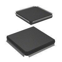
Manufacturer Part Number
D12332VFC25
Description
MCU 3V 0K 144-QFP
Manufacturer
Renesas Electronics America
Series
H8® H8S/2300r
Datasheet
1.DF2338VFC25V.pdf
(1246 pages)
Specifications of D12332VFC25
Core Processor
H8S/2000
Core Size
16-Bit
Speed
25MHz
Connectivity
SCI, SmartCard
Peripherals
DMA, POR, PWM, WDT
Number Of I /o
106
Program Memory Type
ROMless
Ram Size
8K x 8
Voltage - Supply (vcc/vdd)
2.7 V ~ 3.6 V
Data Converters
A/D 12x10b; D/A 4x8b
Oscillator Type
Internal
Operating Temperature
-20°C ~ 75°C
Package / Case
144-QFP
Lead Free Status / RoHS Status
Contains lead / RoHS non-compliant
Eeprom Size
-
Program Memory Size
-
Other names
HD6412332VFC25
HD6412332VFC25
HD6412332VFC25
Available stocks
Company
Part Number
Manufacturer
Quantity
Price
Company:

Part Number:
D12332VFC25V
Manufacturer:
Renesas Electronics America
Quantity:
10 000


Pin
PF
PF
BREQO
PF
Rev.4.00 Sep. 07, 2007 Page 432 of 1210
REJ09B0245-0400
3
2
1
/LWR
/LCAS/
/BACK
Selection Method and Pin Functions
The pin function is switched as shown below according to the operating mode,
bit PF3DDR, and bit LWROD in SYSCR.
The pin function is switched as shown below according to the combination of
the operating mode, and bits RMTS2 to RMTS0, BREQOE, ABW5 to ABW2,
BREQOPS, and PF2DDR.
The pin function is switched as shown below according to the combination of
the operating mode, and bits BRLE and PF1DDR.
Operating
Mode
LWROD
PF3DDR
Pin function
Operating
Mode
[DRAM space
setting] ⋅
[16-bit access
setting]
[BREQOE ⋅
BREQOPS]
PF2DDR
Pin function
Operating
Mode
BRLE
PF1DDR
Pin function
input pin
output pin
input pin
PF
LWR
PF
0
—
0
0
2
1
0
output pin
0
Modes 4 to 6
Modes 4 to 6
PF
output pin
Modes 4 to 6
input pin
0
1
2
PF
PF
0
1
3
1
BREQO
output
1
pin
—
1
output pin
output pin
BACK
PF
—
1
1
output pin
3
LCAS
—
—
1
input pin
input pin
PF
PF
input pin
0
0
3
1
PF
Mode 7
Mode 7
0
2
Mode 7
—
—
—
—
output pin
output pin
output pin
PF
PF
1
PF
1
1
3
1
2
Related parts for D12332VFC25
Image
Part Number
Description
Manufacturer
Datasheet
Request
R

Part Number:
Description:
KIT STARTER FOR M16C/29
Manufacturer:
Renesas Electronics America
Datasheet:

Part Number:
Description:
KIT STARTER FOR R8C/2D
Manufacturer:
Renesas Electronics America
Datasheet:

Part Number:
Description:
R0K33062P STARTER KIT
Manufacturer:
Renesas Electronics America
Datasheet:

Part Number:
Description:
KIT STARTER FOR R8C/23 E8A
Manufacturer:
Renesas Electronics America
Datasheet:

Part Number:
Description:
KIT STARTER FOR R8C/25
Manufacturer:
Renesas Electronics America
Datasheet:

Part Number:
Description:
KIT STARTER H8S2456 SHARPE DSPLY
Manufacturer:
Renesas Electronics America
Datasheet:

Part Number:
Description:
KIT STARTER FOR R8C38C
Manufacturer:
Renesas Electronics America
Datasheet:

Part Number:
Description:
KIT STARTER FOR R8C35C
Manufacturer:
Renesas Electronics America
Datasheet:

Part Number:
Description:
KIT STARTER FOR R8CL3AC+LCD APPS
Manufacturer:
Renesas Electronics America
Datasheet:
Part Number:
Description:
KIT STARTER FOR RX610
Manufacturer:
Renesas Electronics America
Datasheet:

Part Number:
Description:
KIT STARTER FOR R32C/118
Manufacturer:
Renesas Electronics America
Datasheet:

Part Number:
Description:
KIT DEV RSK-R8C/26-29
Manufacturer:
Renesas Electronics America
Datasheet:

Part Number:
Description:
KIT STARTER FOR SH7124
Manufacturer:
Renesas Electronics America
Datasheet:

Part Number:
Description:
KIT STARTER FOR H8SX/1622
Manufacturer:
Renesas Electronics America
Datasheet:

Part Number:
Description:
KIT DEV FOR SH7203
Manufacturer:
Renesas Electronics America
Datasheet: