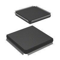
D12332VFC25 Renesas Electronics America, D12332VFC25 Datasheet - Page 204

D12332VFC25
Manufacturer Part Number
D12332VFC25
Description
MCU 3V 0K 144-QFP
Manufacturer
Renesas Electronics America
Series
H8® H8S/2300r
Datasheet
1.DF2338VFC25V.pdf
(1246 pages)
Specifications of D12332VFC25
Core Processor
H8S/2000
Core Size
16-Bit
Speed
25MHz
Connectivity
SCI, SmartCard
Peripherals
DMA, POR, PWM, WDT
Number Of I /o
106
Program Memory Type
ROMless
Ram Size
8K x 8
Voltage - Supply (vcc/vdd)
2.7 V ~ 3.6 V
Data Converters
A/D 12x10b; D/A 4x8b
Oscillator Type
Internal
Operating Temperature
-20°C ~ 75°C
Package / Case
144-QFP
Lead Free Status / RoHS Status
Contains lead / RoHS non-compliant
Eeprom Size
-
Program Memory Size
-
Other names
HD6412332VFC25
HD6412332VFC25
HD6412332VFC25
Available stocks
Company
Part Number
Manufacturer
Quantity
Price
Company:
Part Number:
D12332VFC25V
Manufacturer:
Renesas Electronics America
Quantity:
10 000
- Current page: 204 of 1246
- Download datasheet (7Mb)
Section 6 Bus Controller
6.5.8
Wait Control
There are two ways of inserting wait states in a DRAM access cycle: program wait insertion and
pin wait insertion using the WAIT pin.
Program Wait Insertion: When the bit in ASTCR corresponding to an area designated as DRAM
space is set to 1, from 0 to 3 wait states can be inserted automatically between the T
state and T
c1
c2
state, according to the settings of WCRH and WCRL.
Pin Wait Insertion: When the WAITE bit in BCRH is set to 1, wait input by means of the WAIT
pin is enabled. When DRAM space is accessed in this state, a program wait is first inserted. If the
WAIT pin is low at the falling edge of φ in the last T
or T
state, another T
state is inserted. If
c1
w
w
the WAIT pin is held low, T
states are inserted until it goes high.
w
Figure 6.17 shows an example of wait state insertion timing.
Rev.4.00 Sep. 07, 2007 Page 172 of 1210
REJ09B0245-0400
Related parts for D12332VFC25
Image
Part Number
Description
Manufacturer
Datasheet
Request
R

Part Number:
Description:
KIT STARTER FOR M16C/29
Manufacturer:
Renesas Electronics America
Datasheet:

Part Number:
Description:
KIT STARTER FOR R8C/2D
Manufacturer:
Renesas Electronics America
Datasheet:

Part Number:
Description:
R0K33062P STARTER KIT
Manufacturer:
Renesas Electronics America
Datasheet:

Part Number:
Description:
KIT STARTER FOR R8C/23 E8A
Manufacturer:
Renesas Electronics America
Datasheet:

Part Number:
Description:
KIT STARTER FOR R8C/25
Manufacturer:
Renesas Electronics America
Datasheet:

Part Number:
Description:
KIT STARTER H8S2456 SHARPE DSPLY
Manufacturer:
Renesas Electronics America
Datasheet:

Part Number:
Description:
KIT STARTER FOR R8C38C
Manufacturer:
Renesas Electronics America
Datasheet:

Part Number:
Description:
KIT STARTER FOR R8C35C
Manufacturer:
Renesas Electronics America
Datasheet:

Part Number:
Description:
KIT STARTER FOR R8CL3AC+LCD APPS
Manufacturer:
Renesas Electronics America
Datasheet:

Part Number:
Description:
KIT STARTER FOR RX610
Manufacturer:
Renesas Electronics America
Datasheet:

Part Number:
Description:
KIT STARTER FOR R32C/118
Manufacturer:
Renesas Electronics America
Datasheet:

Part Number:
Description:
KIT DEV RSK-R8C/26-29
Manufacturer:
Renesas Electronics America
Datasheet:

Part Number:
Description:
KIT STARTER FOR SH7124
Manufacturer:
Renesas Electronics America
Datasheet:

Part Number:
Description:
KIT STARTER FOR H8SX/1622
Manufacturer:
Renesas Electronics America
Datasheet:

Part Number:
Description:
KIT DEV FOR SH7203
Manufacturer:
Renesas Electronics America
Datasheet:


