D12332VFC25 Renesas Electronics America, D12332VFC25 Datasheet - Page 53
D12332VFC25
Manufacturer Part Number
D12332VFC25
Description
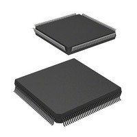
MCU 3V 0K 144-QFP
Manufacturer
Renesas Electronics America
Series
H8® H8S/2300r
Datasheet
1.DF2338VFC25V.pdf
(1246 pages)
Specifications of D12332VFC25
Core Processor
H8S/2000
Core Size
16-Bit
Speed
25MHz
Connectivity
SCI, SmartCard
Peripherals
DMA, POR, PWM, WDT
Number Of I /o
106
Program Memory Type
ROMless
Ram Size
8K x 8
Voltage - Supply (vcc/vdd)
2.7 V ~ 3.6 V
Data Converters
A/D 12x10b; D/A 4x8b
Oscillator Type
Internal
Operating Temperature
-20°C ~ 75°C
Package / Case
144-QFP
Lead Free Status / RoHS Status
Contains lead / RoHS non-compliant
Eeprom Size
-
Program Memory Size
-
Other names
HD6412332VFC25
HD6412332VFC25
HD6412332VFC25
Available stocks
Company
Part Number
Manufacturer
Quantity
Price
Company:

Part Number:
D12332VFC25V
Manufacturer:
Renesas Electronics America
Quantity:
10 000


Type
Bus control
DMA controller
(DMAC)
16-bit timer
pulse unit
(TPU)
Symbol
WAIT
DREQ
DREQ
TEND
TEND
DACK
DACK
TCLKD to
TCLKA
TIOCA
TIOCB
TIOCC
TIOCD
TIOCA
TIOCB
TIOCA
TIOCB
TIOCA
TIOCB
TIOCC
TIOCD
TIOCA
TIOCB
TIOCA
TIOCB
1
0
1
0
1
0
0
0
1
1
2
2
3
3
4
4
5
5
,
0
0
3
3
,
,
,
,
,
,
,
,
,
,
,
,
Pin No.
FP-144G I/O
4,108
134,133
139,138
2,1
125, 127,
129, 130
132 to 129 I/O
128, 127
126, 125
86 to 83
82, 81
80, 79
Input
Input
Output DMA transfer end 1 and 0: These pins indicate
Output DMA transfer acknowledge 1 and 0:
Input
I/O
I/O
I/O
I/O
I/O
Name and Function
Wait: Requests insertion of a wait state in the
bus cycle when accessing external 3-state
address space.
DMA request 1 and 0: These pins request
DMAC activation.
the end of DMAC data transfer.
These are the DMAC single address transfer
acknowledge pins.
Clock input D to A: These pins input an
external clock.
Input capture/output compare match A0 to
D0: The TGR0A to TGR0D input capture input
or output compare output, or PWM output pins.
Input capture/output compare match A1 and
B1: The TGR1A and TGR1B input capture input
or output compare output, or PWM output pins.
Input capture/output compare match A2 and
B2: The TGR2A and TGR2B input capture input
or output compare output, or PWM output pins.
Input capture/output compare match A3 to
D3: The TGR3A to TGR3D input capture input
or output compare output, or PWM output pins.
Input capture/output compare match A4 and
B4: The TGR4A and TGR4B input capture input
or output compare output, or PWM output pins.
Input capture/output compare match A5 and
B5: The TGR5A and TGR5B input capture input
or output compare output, or PWM output pins.
Rev.4.00 Sep. 07, 2007 Page 21 of 1210
REJ09B0245-0400
Related parts for D12332VFC25
Image
Part Number
Description
Manufacturer
Datasheet
Request
R

Part Number:
Description:
KIT STARTER FOR M16C/29
Manufacturer:
Renesas Electronics America
Datasheet:

Part Number:
Description:
KIT STARTER FOR R8C/2D
Manufacturer:
Renesas Electronics America
Datasheet:

Part Number:
Description:
R0K33062P STARTER KIT
Manufacturer:
Renesas Electronics America
Datasheet:

Part Number:
Description:
KIT STARTER FOR R8C/23 E8A
Manufacturer:
Renesas Electronics America
Datasheet:

Part Number:
Description:
KIT STARTER FOR R8C/25
Manufacturer:
Renesas Electronics America
Datasheet:

Part Number:
Description:
KIT STARTER H8S2456 SHARPE DSPLY
Manufacturer:
Renesas Electronics America
Datasheet:

Part Number:
Description:
KIT STARTER FOR R8C38C
Manufacturer:
Renesas Electronics America
Datasheet:

Part Number:
Description:
KIT STARTER FOR R8C35C
Manufacturer:
Renesas Electronics America
Datasheet:

Part Number:
Description:
KIT STARTER FOR R8CL3AC+LCD APPS
Manufacturer:
Renesas Electronics America
Datasheet:
Part Number:
Description:
KIT STARTER FOR RX610
Manufacturer:
Renesas Electronics America
Datasheet:

Part Number:
Description:
KIT STARTER FOR R32C/118
Manufacturer:
Renesas Electronics America
Datasheet:

Part Number:
Description:
KIT DEV RSK-R8C/26-29
Manufacturer:
Renesas Electronics America
Datasheet:

Part Number:
Description:
KIT STARTER FOR SH7124
Manufacturer:
Renesas Electronics America
Datasheet:

Part Number:
Description:
KIT STARTER FOR H8SX/1622
Manufacturer:
Renesas Electronics America
Datasheet:

Part Number:
Description:
KIT DEV FOR SH7203
Manufacturer:
Renesas Electronics America
Datasheet: