D12332VFC25 Renesas Electronics America, D12332VFC25 Datasheet - Page 381
D12332VFC25
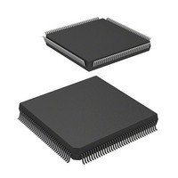
Manufacturer Part Number
D12332VFC25
Description
MCU 3V 0K 144-QFP
Manufacturer
Renesas Electronics America
Series
H8® H8S/2300r
Datasheet
1.DF2338VFC25V.pdf
(1246 pages)
Specifications of D12332VFC25
Core Processor
H8S/2000
Core Size
16-Bit
Speed
25MHz
Connectivity
SCI, SmartCard
Peripherals
DMA, POR, PWM, WDT
Number Of I /o
106
Program Memory Type
ROMless
Ram Size
8K x 8
Voltage - Supply (vcc/vdd)
2.7 V ~ 3.6 V
Data Converters
A/D 12x10b; D/A 4x8b
Oscillator Type
Internal
Operating Temperature
-20°C ~ 75°C
Package / Case
144-QFP
Lead Free Status / RoHS Status
Contains lead / RoHS non-compliant
Eeprom Size
-
Program Memory Size
-
Other names
HD6412332VFC25
HD6412332VFC25
HD6412332VFC25
Available stocks
Company
Part Number
Manufacturer
Quantity
Price
Company:

Part Number:
D12332VFC25V
Manufacturer:
Renesas Electronics America
Quantity:
10 000


Pin
P2
6
/PO
6
/TIOCA
5
Selection Method and Pin Functions
The pin function is switched as shown below according to the combination of
the TPU channel 5 setting (by bits MD3 to MD0 in TMDR5, bits IOA3 to IOA0
in TIOR5, and bits CCLR1 and CCLR0 in TCR5), bit NDER6 in NDERL, and bit
P26DDR.
Notes: 1. TIOCA
TPU Channel
5 Setting
P26DDR
NDER6
Pin function
TPU Channel
5 Setting
MD3 to MD0
IOA3 to IOA0
CCLR1,
CCLR0
Output
function
2. TIOCB
B'0000
B'0100
B'1xxx
5
5
B'0000, B'01xx
Below (1)
input when MD3 to MD0 = B'0000 or B'01xx, and IOA3 = 1.
output is disabled.
(2)
TIOCA
—
—
output
Table
—
—
5
B'0001 to
B'0011
B'0101 to
B'0111
compare
Output
output
(1)
—
Rev.4.00 Sep. 07, 2007 Page 349 of 1210
input
P2
—
B'001x
B'xx00
0
6
(2)
—
—
Table Below (2)
TIOCA
output *
mode 1
B'0010
PWM
(1)
—
output
P2
Other than B'xx00
5
1
0
input *
2
6
than B'01
mode 2
output
REJ09B0245-0400
Other
PWM
(1)
1
B'0011
x: Don't care
output
PO
1
1
B'01
(2)
6
—
Related parts for D12332VFC25
Image
Part Number
Description
Manufacturer
Datasheet
Request
R

Part Number:
Description:
KIT STARTER FOR M16C/29
Manufacturer:
Renesas Electronics America
Datasheet:

Part Number:
Description:
KIT STARTER FOR R8C/2D
Manufacturer:
Renesas Electronics America
Datasheet:

Part Number:
Description:
R0K33062P STARTER KIT
Manufacturer:
Renesas Electronics America
Datasheet:

Part Number:
Description:
KIT STARTER FOR R8C/23 E8A
Manufacturer:
Renesas Electronics America
Datasheet:

Part Number:
Description:
KIT STARTER FOR R8C/25
Manufacturer:
Renesas Electronics America
Datasheet:

Part Number:
Description:
KIT STARTER H8S2456 SHARPE DSPLY
Manufacturer:
Renesas Electronics America
Datasheet:

Part Number:
Description:
KIT STARTER FOR R8C38C
Manufacturer:
Renesas Electronics America
Datasheet:

Part Number:
Description:
KIT STARTER FOR R8C35C
Manufacturer:
Renesas Electronics America
Datasheet:

Part Number:
Description:
KIT STARTER FOR R8CL3AC+LCD APPS
Manufacturer:
Renesas Electronics America
Datasheet:
Part Number:
Description:
KIT STARTER FOR RX610
Manufacturer:
Renesas Electronics America
Datasheet:

Part Number:
Description:
KIT STARTER FOR R32C/118
Manufacturer:
Renesas Electronics America
Datasheet:

Part Number:
Description:
KIT DEV RSK-R8C/26-29
Manufacturer:
Renesas Electronics America
Datasheet:

Part Number:
Description:
KIT STARTER FOR SH7124
Manufacturer:
Renesas Electronics America
Datasheet:

Part Number:
Description:
KIT STARTER FOR H8SX/1622
Manufacturer:
Renesas Electronics America
Datasheet:

Part Number:
Description:
KIT DEV FOR SH7203
Manufacturer:
Renesas Electronics America
Datasheet: