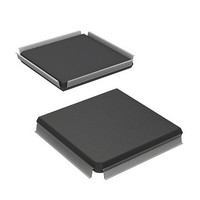
HD6417751RF240V Renesas Electronics America, HD6417751RF240V Datasheet - Page 1216

HD6417751RF240V
Manufacturer Part Number
HD6417751RF240V
Description
MPU 1.5/3.3V 0K PB-FREE 256-QFP
Manufacturer
Renesas Electronics America
Series
SuperH® SH7750r
Datasheet
1.D6417751RBP200DV.pdf
(1226 pages)
Specifications of HD6417751RF240V
Core Processor
SH-4
Core Size
32-Bit
Speed
240MHz
Connectivity
EBI/EMI, FIFO, SCI, SmartCard
Peripherals
DMA, POR, WDT
Number Of I /o
39
Program Memory Type
ROMless
Ram Size
48K x 8
Voltage - Supply (vcc/vdd)
1.4 V ~ 1.6 V
Oscillator Type
External
Operating Temperature
-20°C ~ 75°C
Package / Case
256-QFP Exposed Pad, 256-eQFP, 256-HQFP
Lead Free Status / RoHS Status
Lead free / RoHS Compliant
Eeprom Size
-
Program Memory Size
-
Data Converters
-
Available stocks
Company
Part Number
Manufacturer
Quantity
Price
Company:
Part Number:
HD6417751RF240V
Manufacturer:
Renesas Electronics America
Quantity:
10 000
- Current page: 1216 of 1226
- Download datasheet (7Mb)
G. Power-On and Power-Off Procedures
Notes: 1. Note on Power-On
Rev.4.00 Oct. 10, 2008 Page 1116 of 1122
REJ09B0370-0400
⎯ When the LSI is mounted on a board and connected to other elements, ensure that –0.3 V <
Vin < V
supply V
(min.) and V
shown in figure G.3. The product may be damaged if this time limit is exceeded. It is
recommended that the power-off sequence be completed in as short a time as possible.
2. Workarounds
If the below conditions (A) are not met during power-on, PLL2 may not oscillate
correctly and CKIO may not be output properly.
Conditions (A):
V
or above.
Any of methods (1) to (3) below may be used to avoid the problem by stopping PLL2
oscillation temporarily.
(1) As shown in figure G.1, select mode 6*
(2) After starting with clock operation mode 6*
(3) Temporarily stop PLL2 by writing 0 to FRQCR.PLL2EN. After maintaining
DDQ
desired clock mode once the above conditions (A) are satisfied, and cancel the
power-on reset.
the desired frequency clock.
Note: It is not possible to use frequency divider 1 when this method is employed.
FRQCR.PLL2EN as 0 for 1 µs or more, write 1 to FRQCR.PLL2EN to restart
PLL2.
Note: If this method is used, the clock output from CKIO cannot be guaranteed
until the above operations are completed. If abnormal signal output is produced, the
frequency is higher than normal. Therefore, it is possible that unwanted noise may
be generated from the clock line or, if the LSI’s CKIO pin is used to supply a clock
to another device, the clock may not be supplied correctly to the external device.
When using this method, it is recommended that sufficient verification testing be
performed on the actual system.
DDQ
DD
(V
from the minimum values in the LSI’s guaranteed operation voltage range (V
+ 0.3 V. In addition, the time limit for the fall of power supply V
DDQ
DD
, V
(min.)) to V
DD-CPG
, V
DD-RTC
DDQ
) is 2.0 V or above when V
≥ 1.0 V or V
DD
≥ 0.5 V, respectively, is 150 ms (max.), as
1
immediately after power-on, select the
1
selected, change FRQCR to specify
DD
( V
DD
, V
DD-PLL1
, V
DDQ
DD-PLL2
and power
) is 1.2 V
DDQ
Related parts for HD6417751RF240V
Image
Part Number
Description
Manufacturer
Datasheet
Request
R

Part Number:
Description:
KIT STARTER FOR M16C/29
Manufacturer:
Renesas Electronics America
Datasheet:

Part Number:
Description:
KIT STARTER FOR R8C/2D
Manufacturer:
Renesas Electronics America
Datasheet:

Part Number:
Description:
R0K33062P STARTER KIT
Manufacturer:
Renesas Electronics America
Datasheet:

Part Number:
Description:
KIT STARTER FOR R8C/23 E8A
Manufacturer:
Renesas Electronics America
Datasheet:

Part Number:
Description:
KIT STARTER FOR R8C/25
Manufacturer:
Renesas Electronics America
Datasheet:

Part Number:
Description:
KIT STARTER H8S2456 SHARPE DSPLY
Manufacturer:
Renesas Electronics America
Datasheet:

Part Number:
Description:
KIT STARTER FOR R8C38C
Manufacturer:
Renesas Electronics America
Datasheet:

Part Number:
Description:
KIT STARTER FOR R8C35C
Manufacturer:
Renesas Electronics America
Datasheet:

Part Number:
Description:
KIT STARTER FOR R8CL3AC+LCD APPS
Manufacturer:
Renesas Electronics America
Datasheet:

Part Number:
Description:
KIT STARTER FOR RX610
Manufacturer:
Renesas Electronics America
Datasheet:

Part Number:
Description:
KIT STARTER FOR R32C/118
Manufacturer:
Renesas Electronics America
Datasheet:

Part Number:
Description:
KIT DEV RSK-R8C/26-29
Manufacturer:
Renesas Electronics America
Datasheet:

Part Number:
Description:
KIT STARTER FOR SH7124
Manufacturer:
Renesas Electronics America
Datasheet:

Part Number:
Description:
KIT STARTER FOR H8SX/1622
Manufacturer:
Renesas Electronics America
Datasheet:

Part Number:
Description:
KIT DEV FOR SH7203
Manufacturer:
Renesas Electronics America
Datasheet:


