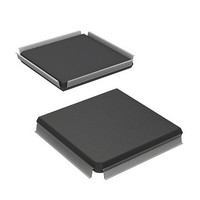
HD6417751RF240V Renesas Electronics America, HD6417751RF240V Datasheet - Page 173

HD6417751RF240V
Manufacturer Part Number
HD6417751RF240V
Description
MPU 1.5/3.3V 0K PB-FREE 256-QFP
Manufacturer
Renesas Electronics America
Series
SuperH® SH7750r
Datasheet
1.D6417751RBP200DV.pdf
(1226 pages)
Specifications of HD6417751RF240V
Core Processor
SH-4
Core Size
32-Bit
Speed
240MHz
Connectivity
EBI/EMI, FIFO, SCI, SmartCard
Peripherals
DMA, POR, WDT
Number Of I /o
39
Program Memory Type
ROMless
Ram Size
48K x 8
Voltage - Supply (vcc/vdd)
1.4 V ~ 1.6 V
Oscillator Type
External
Operating Temperature
-20°C ~ 75°C
Package / Case
256-QFP Exposed Pad, 256-eQFP, 256-HQFP
Lead Free Status / RoHS Status
Lead free / RoHS Compliant
Eeprom Size
-
Program Memory Size
-
Data Converters
-
Available stocks
Company
Part Number
Manufacturer
Quantity
Price
Company:
Part Number:
HD6417751RF240V
Manufacturer:
Renesas Electronics America
Quantity:
10 000
- Current page: 173 of 1226
- Download datasheet (7Mb)
3. Memory Management Unit (MMU)
The area from H'E000 0000 to H'E3FF FFFF comprises addresses for accessing the store queues
(SQs). When the MMU is disabled (MMUCR.AT = 0), the SQ access right is specified by the
MMUCR.SQMD bit. For details, see section 4.7, Store Queues.
The area from H'F000 0000 to H'F0FF FFFF is used for direct access to the instruction cache
address array. For details, see section 4.5.1, IC Address Array.
The area from H'F100 0000 to H'F1FF FFFF is used for direct access to the instruction cache data
array. For details, see section 4.5.2, IC Data Array.
The area from H'F200 0000 to H'F2FF FFFF is used for direct access to the instruction TLB
address array. For details, see section 3.7.1, ITLB Address Array.
The area from H'F300 0000 to H'F3FF FFFF is used for direct access to instruction TLB data
arrays 1 and 2. For details, see sections 3.7.2, ITLB Data Array 1, and 3.7.3, ITLB Data Array 2.
The area from H'F400 0000 to H'F4FF FFFF is used for direct access to the operand cache address
array. For details, see section 4.5.3, OC Address Array.
The area from H'F500 0000 to H'F5FF FFFF is used for direct access to the operand cache data
array. For details, see section 4.5.4, OC Data Array.
The area from H'F600 0000 to H'F6FF FFFF is used for direct access to the unified TLB address
array. For details, see section 3.7.4, UTLB Address Array.
The area from H'F700 0000 to H'F7FF FFFF is used for direct access to unified TLB data arrays 1
and 2. For details, see sections 3.7.5, UTLB Data Array 1, and 3.7.6, UTLB Data Array 2.
The area from H'FC00 0000 to H'FFFF FFFF is the on-chip peripheral module control register
area. For details, see appendix A, Address List.
Rev.4.00 Oct. 10, 2008 Page 73 of 1122
REJ09B0370-0400
Related parts for HD6417751RF240V
Image
Part Number
Description
Manufacturer
Datasheet
Request
R

Part Number:
Description:
KIT STARTER FOR M16C/29
Manufacturer:
Renesas Electronics America
Datasheet:

Part Number:
Description:
KIT STARTER FOR R8C/2D
Manufacturer:
Renesas Electronics America
Datasheet:

Part Number:
Description:
R0K33062P STARTER KIT
Manufacturer:
Renesas Electronics America
Datasheet:

Part Number:
Description:
KIT STARTER FOR R8C/23 E8A
Manufacturer:
Renesas Electronics America
Datasheet:

Part Number:
Description:
KIT STARTER FOR R8C/25
Manufacturer:
Renesas Electronics America
Datasheet:

Part Number:
Description:
KIT STARTER H8S2456 SHARPE DSPLY
Manufacturer:
Renesas Electronics America
Datasheet:

Part Number:
Description:
KIT STARTER FOR R8C38C
Manufacturer:
Renesas Electronics America
Datasheet:

Part Number:
Description:
KIT STARTER FOR R8C35C
Manufacturer:
Renesas Electronics America
Datasheet:

Part Number:
Description:
KIT STARTER FOR R8CL3AC+LCD APPS
Manufacturer:
Renesas Electronics America
Datasheet:

Part Number:
Description:
KIT STARTER FOR RX610
Manufacturer:
Renesas Electronics America
Datasheet:

Part Number:
Description:
KIT STARTER FOR R32C/118
Manufacturer:
Renesas Electronics America
Datasheet:

Part Number:
Description:
KIT DEV RSK-R8C/26-29
Manufacturer:
Renesas Electronics America
Datasheet:

Part Number:
Description:
KIT STARTER FOR SH7124
Manufacturer:
Renesas Electronics America
Datasheet:

Part Number:
Description:
KIT STARTER FOR H8SX/1622
Manufacturer:
Renesas Electronics America
Datasheet:

Part Number:
Description:
KIT DEV FOR SH7203
Manufacturer:
Renesas Electronics America
Datasheet:


