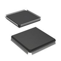
HD6417751RF240V Renesas Electronics America, HD6417751RF240V Datasheet - Page 529

HD6417751RF240V
Manufacturer Part Number
HD6417751RF240V
Description
MPU 1.5/3.3V 0K PB-FREE 256-QFP
Manufacturer
Renesas Electronics America
Series
SuperH® SH7750r
Datasheet
1.D6417751RBP200DV.pdf
(1226 pages)
Specifications of HD6417751RF240V
Core Processor
SH-4
Core Size
32-Bit
Speed
240MHz
Connectivity
EBI/EMI, FIFO, SCI, SmartCard
Peripherals
DMA, POR, WDT
Number Of I /o
39
Program Memory Type
ROMless
Ram Size
48K x 8
Voltage - Supply (vcc/vdd)
1.4 V ~ 1.6 V
Oscillator Type
External
Operating Temperature
-20°C ~ 75°C
Package / Case
256-QFP Exposed Pad, 256-eQFP, 256-HQFP
Lead Free Status / RoHS Status
Lead free / RoHS Compliant
Eeprom Size
-
Program Memory Size
-
Data Converters
-
Available stocks
Company
Part Number
Manufacturer
Quantity
Price
Company:
Part Number:
HD6417751RF240V
Manufacturer:
Renesas Electronics America
Quantity:
10 000
- Current page: 529 of 1226
- Download datasheet (7Mb)
Address Multiplexing: Synchronous DRAM can be connected without external multiplexing
circuitry in accordance with the address multiplex specification bits AMXEXT and AMX2–
AMX0 in MCR. Table 13.15 shows the relationship between the address multiplex specification
bits and the bits output at the address pins. See Appendix E, Synchronous DRAM Address
Multiplexing Tables.
The address signals output at address pins A25–A18, A1, and A0 are not guaranteed.
When A0, the LSB of the synchronous DRAM address, is connected to this LSI, it makes a
longword address specification. Connection should therefore be made in this order: connect pin
A0 of the synchronous DRAM to pin A2 of this LSI, then connect pin A1 to pin A3.
Table 13.15 Example of Correspondence between LSI and Synchronous DRAM Address
A13
A12
A11
A10
A9
A8
A7
A6
A5
A4
A3
A2
A1
A0
Burst Read: The timing chart for a burst read is shown in figure 13.24. In the following example
it is assumed that two 512k × 16-bit × 2-bank synchronous DRAMs are connected, and a 32-bit
data width is used. The burst length is 4. After the Tr cycle in which the ACTV command is
output, a READ command is issued in the Tc1 cycle and, 4 cycles after that, a READA command
is issued and read data is fetched on the rising edge of the external command clock (CKIO) from
cycle Td1 to cycle Td8. The Tpc cycle is used to wait for completion of auto-precharge based on
Pins (32-Bit Bus Width, AMX2–AMX0 = 000, AMXEXT = 0)
LSI Address Pin
A21
A20
A19
A18
A17
A16
A15
A14
A13
A12
A11
A10
Not used
Not used
RAS Cycle
A21
H/L
0
0
A9
A8
A7
A6
A5
A4
A3
A2
Not used
Not used
CAS Cycle
A11
A10
A9
A8
A7
A6
A5
A4
A3
A2
A1
A0
Not used
Not used
Synchronous DRAM Address Pin
Rev.4.00 Oct. 10, 2008 Page 429 of 1122
BANK select bank address
Address precharge setting
Address
13. Bus State Controller (BSC)
Function
REJ09B0370-0400
Related parts for HD6417751RF240V
Image
Part Number
Description
Manufacturer
Datasheet
Request
R

Part Number:
Description:
KIT STARTER FOR M16C/29
Manufacturer:
Renesas Electronics America
Datasheet:

Part Number:
Description:
KIT STARTER FOR R8C/2D
Manufacturer:
Renesas Electronics America
Datasheet:

Part Number:
Description:
R0K33062P STARTER KIT
Manufacturer:
Renesas Electronics America
Datasheet:

Part Number:
Description:
KIT STARTER FOR R8C/23 E8A
Manufacturer:
Renesas Electronics America
Datasheet:

Part Number:
Description:
KIT STARTER FOR R8C/25
Manufacturer:
Renesas Electronics America
Datasheet:

Part Number:
Description:
KIT STARTER H8S2456 SHARPE DSPLY
Manufacturer:
Renesas Electronics America
Datasheet:

Part Number:
Description:
KIT STARTER FOR R8C38C
Manufacturer:
Renesas Electronics America
Datasheet:

Part Number:
Description:
KIT STARTER FOR R8C35C
Manufacturer:
Renesas Electronics America
Datasheet:

Part Number:
Description:
KIT STARTER FOR R8CL3AC+LCD APPS
Manufacturer:
Renesas Electronics America
Datasheet:

Part Number:
Description:
KIT STARTER FOR RX610
Manufacturer:
Renesas Electronics America
Datasheet:

Part Number:
Description:
KIT STARTER FOR R32C/118
Manufacturer:
Renesas Electronics America
Datasheet:

Part Number:
Description:
KIT DEV RSK-R8C/26-29
Manufacturer:
Renesas Electronics America
Datasheet:

Part Number:
Description:
KIT STARTER FOR SH7124
Manufacturer:
Renesas Electronics America
Datasheet:

Part Number:
Description:
KIT STARTER FOR H8SX/1622
Manufacturer:
Renesas Electronics America
Datasheet:

Part Number:
Description:
KIT DEV FOR SH7203
Manufacturer:
Renesas Electronics America
Datasheet:


