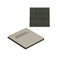
EP4SGX530HH35C2N Altera, EP4SGX530HH35C2N Datasheet - Page 595

EP4SGX530HH35C2N
Manufacturer Part Number
EP4SGX530HH35C2N
Description
IC STRATIX IV FPGA 530K 1152HBGA
Manufacturer
Altera
Series
Stratix® IV GXr
Datasheets
1.EP4SGX110DF29C3N.pdf
(80 pages)
2.EP4SGX110DF29C3N.pdf
(1154 pages)
3.EP4SGX110DF29C3N.pdf
(432 pages)
4.EP4SGX110DF29C3N.pdf
(22 pages)
5.EP4SGX110DF29C3N.pdf
(30 pages)
6.EP4SGX110DF29C3N.pdf
(72 pages)
7.EP4SGX530HH35C2N.pdf
(1145 pages)
Specifications of EP4SGX530HH35C2N
Number Of Logic Elements/cells
531200
Number Of Labs/clbs
21248
Total Ram Bits
27376
Number Of I /o
564
Voltage - Supply
0.87 V ~ 0.93 V
Mounting Type
Surface Mount
Operating Temperature
0°C ~ 85°C
Package / Case
1152-HBGA
Family Name
Stratix® IV
Number Of Logic Blocks/elements
531200
# Registers
424960
# I/os (max)
560
Process Technology
40nm
Operating Supply Voltage (typ)
900mV
Logic Cells
531200
Ram Bits
28033024
Operating Supply Voltage (min)
0.87V
Operating Supply Voltage (max)
0.93V
Operating Temp Range
0C to 85C
Operating Temperature Classification
Commercial
Mounting
Surface Mount
Pin Count
1152
Package Type
FCHBGA
Lead Free Status / RoHS Status
Lead free / RoHS Compliant
Number Of Gates
-
Lead Free Status / Rohs Status
Compliant
Available stocks
Company
Part Number
Manufacturer
Quantity
Price
- EP4SGX110DF29C3N PDF datasheet
- EP4SGX110DF29C3N PDF datasheet #2
- EP4SGX110DF29C3N PDF datasheet #3
- EP4SGX110DF29C3N PDF datasheet #4
- EP4SGX110DF29C3N PDF datasheet #5
- EP4SGX110DF29C3N PDF datasheet #6
- EP4SGX530HH35C2N PDF datasheet #7
- Current page: 595 of 1154
- Download datasheet (32Mb)
Chapter 1: Transceiver Architecture in Stratix IV Devices
Transceiver Block Architecture
February 2011 Altera Corporation
1
Fundamental reset is provided by the system to the component or adapter card using
the auxiliary signal PERST#. The PCIe Base Specification 2.0 specifies that PERST# must
be kept asserted for a minimum of 100 ms (TPVPERL) after the system power becomes
stable in a cold reset situation. Additionally, all system components must enter the
LTSSM Detect state within 20 ms and the link must become active within 100 ms after
de-assertion of the PERST# signal. This implies that each PCIe system component must
become active within 200 ms after the power becomes stable.
The link being active is interpreted as the physical layer device coming out of
electrical idle in the L0 state of the LTSSM state machine.
Figure 1–120
Figure 1–120. PCIe Cold Reset Requirements
The time taken by a PCIe port implemented using the Stratix IV GX and GT device to
go from power up to link active state is described below:
■
■
■
To meet the PCIe specification of 200 ms from power on to link active, the
Stratix IV GX and GT device configuration time must be less than 148 ms
(200 ms –12 ms for power on reset and -40 ms for the link to become active after
PERST# de-assertion).
Power on reset (POR)—begins after power rails become stable. Typically takes
12 ms
FPGA configuration/programming—begins after POR. Configuration time
depends on the FPGA density
Time taken from de-assertion of PERST# to link active—typically takes 40 ms
(pending characterization and verification of PCIe soft IP and hard IP)
Power Rail
PERST#
lists the PCIe cold reset timing requirements.
1
T
PVPERL
100 ms
2
d" 20 ms
T
2-3
d" 100 ms
T
3
2-4
4
Stratix IV Device Handbook Volume 2: Transceivers
Marker 1: Power becomes stable
Marker 2: PERST# gets de-asserted
Marker 3: Maximum time for Marker 2 for
the LTSSM to enter the Detect state
Marker 4: Maximum time for Marker 2 for
the link to become active
1–151
Related parts for EP4SGX530HH35C2N
Image
Part Number
Description
Manufacturer
Datasheet
Request
R

Part Number:
Description:
CYCLONE II STARTER KIT EP2C20N
Manufacturer:
Altera
Datasheet:

Part Number:
Description:
CPLD, EP610 Family, ECMOS Process, 300 Gates, 16 Macro Cells, 16 Reg., 16 User I/Os, 5V Supply, 35 Speed Grade, 24DIP
Manufacturer:
Altera Corporation
Datasheet:

Part Number:
Description:
CPLD, EP610 Family, ECMOS Process, 300 Gates, 16 Macro Cells, 16 Reg., 16 User I/Os, 5V Supply, 15 Speed Grade, 24DIP
Manufacturer:
Altera Corporation
Datasheet:

Part Number:
Description:
Manufacturer:
Altera Corporation
Datasheet:

Part Number:
Description:
CPLD, EP610 Family, ECMOS Process, 300 Gates, 16 Macro Cells, 16 Reg., 16 User I/Os, 5V Supply, 30 Speed Grade, 24DIP
Manufacturer:
Altera Corporation
Datasheet:

Part Number:
Description:
High-performance, low-power erasable programmable logic devices with 8 macrocells, 10ns
Manufacturer:
Altera Corporation
Datasheet:

Part Number:
Description:
High-performance, low-power erasable programmable logic devices with 8 macrocells, 7ns
Manufacturer:
Altera Corporation
Datasheet:

Part Number:
Description:
Classic EPLD
Manufacturer:
Altera Corporation
Datasheet:

Part Number:
Description:
High-performance, low-power erasable programmable logic devices with 8 macrocells, 10ns
Manufacturer:
Altera Corporation
Datasheet:

Part Number:
Description:
Manufacturer:
Altera Corporation
Datasheet:

Part Number:
Description:
Manufacturer:
Altera Corporation
Datasheet:

Part Number:
Description:
Manufacturer:
Altera Corporation
Datasheet:

Part Number:
Description:
CPLD, EP610 Family, ECMOS Process, 300 Gates, 16 Macro Cells, 16 Reg., 16 User I/Os, 5V Supply, 25 Speed Grade, 24DIP
Manufacturer:
Altera Corporation
Datasheet:


