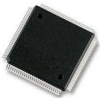
MC9S12E128CPV Freescale Semiconductor, MC9S12E128CPV Datasheet - Page 138

MC9S12E128CPV
Manufacturer Part Number
MC9S12E128CPV
Description
Microcontrollers (MCU) 16 Bit 16MHz
Manufacturer
Freescale Semiconductor
Datasheet
1.MC9S12E128CPV.pdf
(606 pages)
Specifications of MC9S12E128CPV
Data Bus Width
16 bit
Program Memory Type
Flash
Program Memory Size
128 KB
Data Ram Size
8 KB
Interface Type
SCI, SPI
Maximum Clock Frequency
25 MHz
Number Of Programmable I/os
92
Number Of Timers
16 bit
Operating Supply Voltage
3.135 V to 5.5 V
Maximum Operating Temperature
+ 85 C
Mounting Style
SMD/SMT
Package / Case
LQFP-112
Minimum Operating Temperature
- 40 C
On-chip Adc
10 bit
On-chip Dac
8 bit, 2 Channel
Lead Free Status / Rohs Status
No RoHS Version Available
Available stocks
Company
Part Number
Manufacturer
Quantity
Price
Company:
Part Number:
MC9S12E128CPVE
Manufacturer:
Freescale Semiconductor
Quantity:
10 000
- Current page: 138 of 606
- Download datasheet (4Mb)
Chapter 3 Port Integration Module (PIM9E128V1)
Read: Anytime. Write: Never, writes to this register have no effect.
This register always reads back the status of the associated pins.
3.3.2.3
Read: Anytime. Write: Anytime.
This register configures port pins PM[7:3] and PM[1:0] as either input or output.
If the IIC is enabled, the IIC controls the SCL and SDA I/O direction, and the corresponding DDRM[7:6]
bits have no effect on their I/O direction. Refer to the IIC block description chapter for details.
If the SCI2 transmitter is enabled, the I/O direction of the transmit pin TXD2 is controlled by SCI2, and
the DDRM5 bit has no effect. If the SCI2 receiver is enabled, the I/O direction of the receive pin RXD2 is
controlled by SCI2, and the DDRM4 bit has no effect. Refer to the SCI block description chapter for
further details.
If the DAC1 or DAC0 channel is enabled, the associated pin DAO1 or DAO0 is forced to be output, and
the associated DDRM1 or DDRM0 bit has no effect.
The DDRM bits do not change to reflect the pin I/O direction when not being used as GPIO. The
DDRM[7:3]; DDRM[1:0] bits revert to controlling the I/O direction of the pins when the associated IIC,
SCI, or DAC1/0 function are disabled.
138
DDRM[7:3,
7:3, 1:0
Reset
Field
1:0]
W
R
DDRM7
Data Direction Port M
0 Associated pin is configured as input.
1 Associated pin is configured as output.
Port M Data Direction Register (DDRM)
0
7
= Reserved or Unimplemented
DDRM6
0
6
Figure 3-12. Port M Data Direction Register (DDRM)
Table 3-9. DDRM Field Descriptions
DDRM5
MC9S12E128 Data Sheet, Rev. 1.07
0
5
DDRM4
0
4
Description
DDRM3
0
3
0
0
2
DDRM1
Freescale Semiconductor
0
1
DDRM0
0
0
Related parts for MC9S12E128CPV
Image
Part Number
Description
Manufacturer
Datasheet
Request
R
Part Number:
Description:
Manufacturer:
Freescale Semiconductor, Inc
Datasheet:
Part Number:
Description:
Manufacturer:
Freescale Semiconductor, Inc
Datasheet:
Part Number:
Description:
Manufacturer:
Freescale Semiconductor, Inc
Datasheet:
Part Number:
Description:
Manufacturer:
Freescale Semiconductor, Inc
Datasheet:
Part Number:
Description:
Manufacturer:
Freescale Semiconductor, Inc
Datasheet:
Part Number:
Description:
Manufacturer:
Freescale Semiconductor, Inc
Datasheet:
Part Number:
Description:
Manufacturer:
Freescale Semiconductor, Inc
Datasheet:
Part Number:
Description:
Manufacturer:
Freescale Semiconductor, Inc
Datasheet:
Part Number:
Description:
Manufacturer:
Freescale Semiconductor, Inc
Datasheet:
Part Number:
Description:
Manufacturer:
Freescale Semiconductor, Inc
Datasheet:
Part Number:
Description:
Manufacturer:
Freescale Semiconductor, Inc
Datasheet:
Part Number:
Description:
Manufacturer:
Freescale Semiconductor, Inc
Datasheet:
Part Number:
Description:
Manufacturer:
Freescale Semiconductor, Inc
Datasheet:
Part Number:
Description:
Manufacturer:
Freescale Semiconductor, Inc
Datasheet:
Part Number:
Description:
Manufacturer:
Freescale Semiconductor, Inc
Datasheet:


