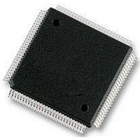
MC9S12E128CPV Freescale Semiconductor, MC9S12E128CPV Datasheet - Page 362

MC9S12E128CPV
Manufacturer Part Number
MC9S12E128CPV
Description
Microcontrollers (MCU) 16 Bit 16MHz
Manufacturer
Freescale Semiconductor
Datasheet
1.MC9S12E128CPV.pdf
(606 pages)
Specifications of MC9S12E128CPV
Data Bus Width
16 bit
Program Memory Type
Flash
Program Memory Size
128 KB
Data Ram Size
8 KB
Interface Type
SCI, SPI
Maximum Clock Frequency
25 MHz
Number Of Programmable I/os
92
Number Of Timers
16 bit
Operating Supply Voltage
3.135 V to 5.5 V
Maximum Operating Temperature
+ 85 C
Mounting Style
SMD/SMT
Package / Case
LQFP-112
Minimum Operating Temperature
- 40 C
On-chip Adc
10 bit
On-chip Dac
8 bit, 2 Channel
Lead Free Status / Rohs Status
No RoHS Version Available
Available stocks
Company
Part Number
Manufacturer
Quantity
Price
Company:
Part Number:
MC9S12E128CPVE
Manufacturer:
Freescale Semiconductor
Quantity:
10 000
- Current page: 362 of 606
- Download datasheet (4Mb)
Chapter 11 Pulse Width Modulator with Fault Protection (PMF15B6CV2)
In complementary channel operation, there are three additional features:
11.4.5
While in the complementary mode, each PWM pair can be used to drive top/bottom transistors, as shown
in
active, the bottom PWM channel is inactive, and vice versa.
Deadtime generators automatically insert software-selectable activation delays into each pair of PWM
outputs. The deadtime register (PMFDTMx) specifies the number of PWM clock cycles to use for
deadtime delay. Every time the deadtime generator inputs changes state, deadtime is inserted. Deadtime
forces both PWM outputs in the pair to the inactive state.
A method of correcting this, adding to or subtracting from the PWM value used, is discussed next.
362
Figure
GENERATOR
•
•
•
•
PWM
Deadtime insertion
Separate top and bottom pulse width correction for distortions are caused by deadtime inserted and
the motor drive characteristics
Separate top and bottom output polarity control
Swap functionality
11-49. Ideally, the PWM pairs are an inversion of each other. When the top PWM channel is
Deadtime Generators
To avoid a short-circuit on the DC bus and endangering the transistor, there
must be no overlap of conducting intervals between top and bottom
transistor. But the transistor’s characteristics make its switching-off time
longer than switching-on time. To avoid the conducting overlap of top and
bottom transistors, deadtime needs to be inserted in the switching period.
CURRENT
STATUS
PWM0 &
PWM1
PWM2 &
PWM3
PWM4 &
PWM5
OUT0
OUT2
OUT4
Figure 11-49. Deadtime Generators
MC9S12E128 Data Sheet, Rev. 1.07
OUTCTL0
OUTCTL2
OUTCTL4
MUX
MUX
MUX
NOTE
GENERATOR
GENERATOR
GENERATOR
DEADTIME
DEADTIME
DEADTIME
OUT1
OUT3
OUT5
TOP/BOTTOM
TOP/BOTTOM
TOP/BOTTOM
GENERATOR
GENERATOR
GENERATOR
TOP (PWM0)
BOTTOM (PWM1)
TOP (PWM2)
BOTTOM (PWM3)
TOP (PWM4)
BOTTOM (PWM5)
Freescale Semiconductor
TO FAULT
PROTECTION
TO FAULT
PROTECTION
TO FAULT
PROTECTION
Related parts for MC9S12E128CPV
Image
Part Number
Description
Manufacturer
Datasheet
Request
R
Part Number:
Description:
Manufacturer:
Freescale Semiconductor, Inc
Datasheet:
Part Number:
Description:
Manufacturer:
Freescale Semiconductor, Inc
Datasheet:
Part Number:
Description:
Manufacturer:
Freescale Semiconductor, Inc
Datasheet:
Part Number:
Description:
Manufacturer:
Freescale Semiconductor, Inc
Datasheet:
Part Number:
Description:
Manufacturer:
Freescale Semiconductor, Inc
Datasheet:
Part Number:
Description:
Manufacturer:
Freescale Semiconductor, Inc
Datasheet:
Part Number:
Description:
Manufacturer:
Freescale Semiconductor, Inc
Datasheet:
Part Number:
Description:
Manufacturer:
Freescale Semiconductor, Inc
Datasheet:
Part Number:
Description:
Manufacturer:
Freescale Semiconductor, Inc
Datasheet:
Part Number:
Description:
Manufacturer:
Freescale Semiconductor, Inc
Datasheet:
Part Number:
Description:
Manufacturer:
Freescale Semiconductor, Inc
Datasheet:
Part Number:
Description:
Manufacturer:
Freescale Semiconductor, Inc
Datasheet:
Part Number:
Description:
Manufacturer:
Freescale Semiconductor, Inc
Datasheet:
Part Number:
Description:
Manufacturer:
Freescale Semiconductor, Inc
Datasheet:
Part Number:
Description:
Manufacturer:
Freescale Semiconductor, Inc
Datasheet:


