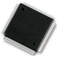
MC9S12E128CPV Freescale Semiconductor, MC9S12E128CPV Datasheet - Page 273

MC9S12E128CPV
Manufacturer Part Number
MC9S12E128CPV
Description
Microcontrollers (MCU) 16 Bit 16MHz
Manufacturer
Freescale Semiconductor
Datasheet
1.MC9S12E128CPV.pdf
(606 pages)
Specifications of MC9S12E128CPV
Data Bus Width
16 bit
Program Memory Type
Flash
Program Memory Size
128 KB
Data Ram Size
8 KB
Interface Type
SCI, SPI
Maximum Clock Frequency
25 MHz
Number Of Programmable I/os
92
Number Of Timers
16 bit
Operating Supply Voltage
3.135 V to 5.5 V
Maximum Operating Temperature
+ 85 C
Mounting Style
SMD/SMT
Package / Case
LQFP-112
Minimum Operating Temperature
- 40 C
On-chip Adc
10 bit
On-chip Dac
8 bit, 2 Channel
Lead Free Status / Rohs Status
No RoHS Version Available
Available stocks
Company
Part Number
Manufacturer
Quantity
Price
Company:
Part Number:
MC9S12E128CPVE
Manufacturer:
Freescale Semiconductor
Quantity:
10 000
- Current page: 273 of 606
- Download datasheet (4Mb)
8.4.5.6.1
In this wakeup method, an idle condition on the RXD pin clears the RWU bit and wakes up the SCI. The
initial frame or frames of every message contain addressing information. All receivers evaluate the
addressing information, and receivers for which the message is addressed process the frames that follow.
Any receiver for which a message is not addressed can set its RWU bit and return to the standby state. The
RWU bit remains set and the receiver remains on standby until another idle character appears on the RXD
pin.
Idle line wakeup requires that messages be separated by at least one idle character and that no message
contains idle characters.
The idle character that wakes a receiver does not set the receiver idle bit, IDLE, or the receive data register
full flag, RDRF.
The idle line type bit, ILT, determines whether the receiver begins counting logic 1s as idle character bits
after the start bit or after the stop bit. ILT is in SCI control register 1 (SCICR1).
8.4.5.6.2
In this wakeup method, a logic 1 in the most significant bit (MSB) position of a frame clears the RWU bit
and wakes up the SCI. The logic 1 in the MSB position marks a frame as an address frame that contains
addressing information. All receivers evaluate the addressing information, and the receivers for which the
message is addressed process the frames that follow. Any receiver for which a message is not addressed
can set its RWU bit and return to the standby state. The RWU bit remains set and the receiver remains on
standby until another address frame appears on the RXD pin.
The logic 1 MSB of an address frame clears the receiver’s RWU bit before the stop bit is received and sets
the RDRF flag.
Address mark wakeup allows messages to contain idle characters but requires that the MSB be reserved
for use in address frames.
8.4.6
Normally, the SCI uses two pins for transmitting and receiving. In single-wire operation, the RXD pin is
disconnected from the SCI. The SCI uses the TXD pin for both receiving and transmitting.
Freescale Semiconductor
Single-Wire Operation
Idle Input Line Wakeup (WAKE = 0)
Address Mark Wakeup (WAKE = 1)
With the WAKE bit clear, setting the RWU bit after the RXD pin has been
idle can cause the receiver to wake up immediately.
Figure 8-24. Single-Wire Operation (LOOPS = 1, RSRC = 1)
TRANSMITTER
RECEIVER
MC9S12E128 Data Sheet, Rev. 1.07
NOTE
Chapter 8 Serial Communication Interface (SCIV3)
RXD
TXD
273
Related parts for MC9S12E128CPV
Image
Part Number
Description
Manufacturer
Datasheet
Request
R
Part Number:
Description:
Manufacturer:
Freescale Semiconductor, Inc
Datasheet:
Part Number:
Description:
Manufacturer:
Freescale Semiconductor, Inc
Datasheet:
Part Number:
Description:
Manufacturer:
Freescale Semiconductor, Inc
Datasheet:
Part Number:
Description:
Manufacturer:
Freescale Semiconductor, Inc
Datasheet:
Part Number:
Description:
Manufacturer:
Freescale Semiconductor, Inc
Datasheet:
Part Number:
Description:
Manufacturer:
Freescale Semiconductor, Inc
Datasheet:
Part Number:
Description:
Manufacturer:
Freescale Semiconductor, Inc
Datasheet:
Part Number:
Description:
Manufacturer:
Freescale Semiconductor, Inc
Datasheet:
Part Number:
Description:
Manufacturer:
Freescale Semiconductor, Inc
Datasheet:
Part Number:
Description:
Manufacturer:
Freescale Semiconductor, Inc
Datasheet:
Part Number:
Description:
Manufacturer:
Freescale Semiconductor, Inc
Datasheet:
Part Number:
Description:
Manufacturer:
Freescale Semiconductor, Inc
Datasheet:
Part Number:
Description:
Manufacturer:
Freescale Semiconductor, Inc
Datasheet:
Part Number:
Description:
Manufacturer:
Freescale Semiconductor, Inc
Datasheet:
Part Number:
Description:
Manufacturer:
Freescale Semiconductor, Inc
Datasheet:


