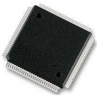
MC9S12E128CPV Freescale Semiconductor, MC9S12E128CPV Datasheet - Page 293

MC9S12E128CPV
Manufacturer Part Number
MC9S12E128CPV
Description
Microcontrollers (MCU) 16 Bit 16MHz
Manufacturer
Freescale Semiconductor
Datasheet
1.MC9S12E128CPV.pdf
(606 pages)
Specifications of MC9S12E128CPV
Data Bus Width
16 bit
Program Memory Type
Flash
Program Memory Size
128 KB
Data Ram Size
8 KB
Interface Type
SCI, SPI
Maximum Clock Frequency
25 MHz
Number Of Programmable I/os
92
Number Of Timers
16 bit
Operating Supply Voltage
3.135 V to 5.5 V
Maximum Operating Temperature
+ 85 C
Mounting Style
SMD/SMT
Package / Case
LQFP-112
Minimum Operating Temperature
- 40 C
On-chip Adc
10 bit
On-chip Dac
8 bit, 2 Channel
Lead Free Status / Rohs Status
No RoHS Version Available
Available stocks
Company
Part Number
Manufacturer
Quantity
Price
Company:
Part Number:
MC9S12E128CPVE
Manufacturer:
Freescale Semiconductor
Quantity:
10 000
- Current page: 293 of 606
- Download datasheet (4Mb)
9.4.4
Baud rate generation consists of a series of divider stages. Six bits in the SPI Baud Rate register (SPPR2,
SPPR1, SPPR0, SPR2, SPR1, and SPR0) determine the divisor to the SPI module clock which results in
the SPI baud rate.
The SPI clock rate is determined by the product of the value in the baud rate preselection bits
(SPPR2–SPPR0) and the value in the baud rate selection bits (SPR2–SPR0). The module clock divisor
equation is shown in
When all bits are clear (the default condition), the SPI module clock is divided by 2. When the selection
bits (SPR2–SPR0) are 001 and the preselection bits (SPPR2–SPPR0) are 000, the module clock divisor
becomes 4. When the selection bits are 010, the module clock divisor becomes 8 etc.
When the preselection bits are 001, the divisor determined by the selection bits is multiplied by 2. When
the preselection bits are 010, the divisor is multiplied by 3, etc. See
all bit conditions, based on a 25-MHz bus clock. The two sets of selects allows the clock to be divided by
a non-power of two to achieve other baud rates such as divide by 6, divide by 10, etc.
Freescale Semiconductor
End of Idle State
SCK Edge Nr.
MSB first (LSBFE = 0):
SCK (CPOL = 0)
SCK (CPOL = 1)
SAMPLE I
MOSI/MISO
CHANGE O
CHANGE O
SEL SS (O)
Master only
SEL SS (I)
t
t
t
MOSI pin
MISO pin
LSB first (LSBFE = 1):
L
T
I
= Minimum idling time between transfers (minimum SS high time), not required for back to back transfers
= Minimum leading time before the first SCK edge, not required for back to back transfers
= Minimum trailing time after the last SCK edge
SPI Baud Rate Generation
Figure 9-11
tL
1
MSB
LSB
2
Figure 9-10. SPI Clock Format 1 (CPHA = 1)
3
Begin
Bit 6
Bit 1
4
MC9S12E128 Data Sheet, Rev. 1.07
5
Bit 5
Bit 2
6
7
Bit 4
Bit 3
8
Transfer
9
Bit 3
Bit 4
10
11
Bit 2
Bit 5
12
Table 9-7
13 14
Chapter 9 Serial Peripheral Interface (SPIV3)
Bit 1
Bit 6
End
15
for baud rate calculations for
MSB
LSB
16
tT
Minimum 1/2 SCK
Begin of Idle State
tI
for t
T
tL
, t
l
, t
L
293
Related parts for MC9S12E128CPV
Image
Part Number
Description
Manufacturer
Datasheet
Request
R
Part Number:
Description:
Manufacturer:
Freescale Semiconductor, Inc
Datasheet:
Part Number:
Description:
Manufacturer:
Freescale Semiconductor, Inc
Datasheet:
Part Number:
Description:
Manufacturer:
Freescale Semiconductor, Inc
Datasheet:
Part Number:
Description:
Manufacturer:
Freescale Semiconductor, Inc
Datasheet:
Part Number:
Description:
Manufacturer:
Freescale Semiconductor, Inc
Datasheet:
Part Number:
Description:
Manufacturer:
Freescale Semiconductor, Inc
Datasheet:
Part Number:
Description:
Manufacturer:
Freescale Semiconductor, Inc
Datasheet:
Part Number:
Description:
Manufacturer:
Freescale Semiconductor, Inc
Datasheet:
Part Number:
Description:
Manufacturer:
Freescale Semiconductor, Inc
Datasheet:
Part Number:
Description:
Manufacturer:
Freescale Semiconductor, Inc
Datasheet:
Part Number:
Description:
Manufacturer:
Freescale Semiconductor, Inc
Datasheet:
Part Number:
Description:
Manufacturer:
Freescale Semiconductor, Inc
Datasheet:
Part Number:
Description:
Manufacturer:
Freescale Semiconductor, Inc
Datasheet:
Part Number:
Description:
Manufacturer:
Freescale Semiconductor, Inc
Datasheet:
Part Number:
Description:
Manufacturer:
Freescale Semiconductor, Inc
Datasheet:


