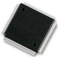
MC9S12E128CPV Freescale Semiconductor, MC9S12E128CPV Datasheet - Page 204

MC9S12E128CPV
Manufacturer Part Number
MC9S12E128CPV
Description
Microcontrollers (MCU) 16 Bit 16MHz
Manufacturer
Freescale Semiconductor
Datasheet
1.MC9S12E128CPV.pdf
(606 pages)
Specifications of MC9S12E128CPV
Data Bus Width
16 bit
Program Memory Type
Flash
Program Memory Size
128 KB
Data Ram Size
8 KB
Interface Type
SCI, SPI
Maximum Clock Frequency
25 MHz
Number Of Programmable I/os
92
Number Of Timers
16 bit
Operating Supply Voltage
3.135 V to 5.5 V
Maximum Operating Temperature
+ 85 C
Mounting Style
SMD/SMT
Package / Case
LQFP-112
Minimum Operating Temperature
- 40 C
On-chip Adc
10 bit
On-chip Dac
8 bit, 2 Channel
Lead Free Status / Rohs Status
No RoHS Version Available
Available stocks
Company
Part Number
Manufacturer
Quantity
Price
Company:
Part Number:
MC9S12E128CPVE
Manufacturer:
Freescale Semiconductor
Quantity:
10 000
- Current page: 204 of 606
- Download datasheet (4Mb)
Chapter 5 Oscillator (OSCV2)
5.3
The CRG contains the registers and associated bits for controlling and monitoring the OSCV2 module.
5.4
The OSCV2 block has two external pins, EXTAL and XTAL. The oscillator input pin, EXTAL, is intended
to be connected to either a crystal or an external clock source. The selection of Colpitts oscillator or Pierce
oscillator/external clock depends on the XCLKS signal which is sampled during reset. The XTAL pin is
an output signal that provides crystal circuit feedback.
A buffered EXTAL signal, OSCCLK, becomes the internal reference clock. To improve noise immunity,
the oscillator is powered by the V
The Pierce oscillator can be used for higher frequencies compared to the low power Colpitts oscillator.
5.4.1
The Colpitts oscillator is equipped with a feedback system which does not waste current by generating
harmonics. Its configuration is “Colpitts oscillator with translated ground.” The transconductor used is
driven by a current source under the control of a peak detector which will measure the amplitude of the
AC signal appearing on EXTAL node in order to implement an amplitude limitation control (ALC) loop.
The ALC loop is in charge of reducing the quiescent current in the transconductor as a result of an increase
in the oscillation amplitude. The oscillation amplitude can be limited to two values. The normal amplitude
which is intended for non power saving modes and a small amplitude which is intended for low power
operation modes. Please refer to the CRG block description chapter for the control and assignment of the
amplitude value to operation modes.
5.4.2
The clock monitor circuit is based on an internal resistor-capacitor (RC) time delay so that it can operate
without any MCU clocks. If no OSCCLK edges are detected within this RC time delay, the clock monitor
indicates a failure which asserts self clock mode or generates a system reset depending on the state of
SCME bit. If the clock monitor is disabled or the presence of clocks is detected no failure is indicated.The
clock monitor function is enabled/disabled by the CME control bit, described in the CRG block description
chapter.
5.5
OSCV2 contains a clock monitor, which can trigger an interrupt or reset. The control bits and status bits
for the clock monitor are described in the CRG block description chapter.
204
Memory Map and Register Definition
Functional Description
Interrupts
Amplitude Limitation Control (ALC)
Clock Monitor (CM)
DDPLL
MC9S12E128 Data Sheet, Rev. 1.07
and V
SSPLL
power supply pins.
Freescale Semiconductor
Related parts for MC9S12E128CPV
Image
Part Number
Description
Manufacturer
Datasheet
Request
R
Part Number:
Description:
Manufacturer:
Freescale Semiconductor, Inc
Datasheet:
Part Number:
Description:
Manufacturer:
Freescale Semiconductor, Inc
Datasheet:
Part Number:
Description:
Manufacturer:
Freescale Semiconductor, Inc
Datasheet:
Part Number:
Description:
Manufacturer:
Freescale Semiconductor, Inc
Datasheet:
Part Number:
Description:
Manufacturer:
Freescale Semiconductor, Inc
Datasheet:
Part Number:
Description:
Manufacturer:
Freescale Semiconductor, Inc
Datasheet:
Part Number:
Description:
Manufacturer:
Freescale Semiconductor, Inc
Datasheet:
Part Number:
Description:
Manufacturer:
Freescale Semiconductor, Inc
Datasheet:
Part Number:
Description:
Manufacturer:
Freescale Semiconductor, Inc
Datasheet:
Part Number:
Description:
Manufacturer:
Freescale Semiconductor, Inc
Datasheet:
Part Number:
Description:
Manufacturer:
Freescale Semiconductor, Inc
Datasheet:
Part Number:
Description:
Manufacturer:
Freescale Semiconductor, Inc
Datasheet:
Part Number:
Description:
Manufacturer:
Freescale Semiconductor, Inc
Datasheet:
Part Number:
Description:
Manufacturer:
Freescale Semiconductor, Inc
Datasheet:
Part Number:
Description:
Manufacturer:
Freescale Semiconductor, Inc
Datasheet:


