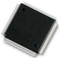
MC9S12E128CPV Freescale Semiconductor, MC9S12E128CPV Datasheet - Page 555

MC9S12E128CPV
Manufacturer Part Number
MC9S12E128CPV
Description
Microcontrollers (MCU) 16 Bit 16MHz
Manufacturer
Freescale Semiconductor
Datasheet
1.MC9S12E128CPV.pdf
(606 pages)
Specifications of MC9S12E128CPV
Data Bus Width
16 bit
Program Memory Type
Flash
Program Memory Size
128 KB
Data Ram Size
8 KB
Interface Type
SCI, SPI
Maximum Clock Frequency
25 MHz
Number Of Programmable I/os
92
Number Of Timers
16 bit
Operating Supply Voltage
3.135 V to 5.5 V
Maximum Operating Temperature
+ 85 C
Mounting Style
SMD/SMT
Package / Case
LQFP-112
Minimum Operating Temperature
- 40 C
On-chip Adc
10 bit
On-chip Dac
8 bit, 2 Channel
Lead Free Status / Rohs Status
No RoHS Version Available
Available stocks
Company
Part Number
Manufacturer
Quantity
Price
Company:
Part Number:
MC9S12E128CPVE
Manufacturer:
Freescale Semiconductor
Quantity:
10 000
- Current page: 555 of 606
- Download datasheet (4Mb)
The HCS12 core architecture limits the physical address space available to 64K bytes. The program page
index register allows for integrating up to 1M byte of FLASH or ROM into the system by using the six
page index bits to page 16K byte blocks into the program page window located from 0x8000 to 0xBFFF
as defined in
without using the address bus.
19.4
The MMC sub-block performs four basic functions of the core operation: bus control, address decoding
and select signal generation, memory expansion, and security decoding for the system. Each aspect is
described in the following subsections.
19.4.1
The MMC controls the address bus and data buses that interface the core with the rest of the system. This
includes the multiplexing of the input data buses to the core onto the main CPU read data bus and control
Freescale Semiconductor
PIX[5:0]
Field
5:0
Functional Description
Bus Control
Table
Program Page Index Bits 5:0 — These page index bits are used to select which of the 64 FLASH or ROM
array pages is to be accessed in the program page window as shown in
Normal writes to this register take one cycle to go into effect. Writes to this
register using the special access of the CALL and RTC instructions will be
complete before the end of the associated instruction.
PIX5
0
0
0
0
1
1
1
1
.
.
.
.
.
19-14. CALL and RTC instructions have special access to read and write this register
PIX4
0
0
0
0
1
1
1
1
.
.
.
.
.
Table 19-14. Program Page Index Register Bits
Table 19-13. MEMSIZ0 Field Descriptions
PIX3
0
0
0
0
1
1
1
1
.
.
.
.
MC9S12E128 Data Sheet, Rev. 1.07
PIX2
0
0
0
0
1
1
1
1
.
.
.
.
.
NOTE
PIX1
Description
0
0
1
1
0
0
1
1
.
.
.
.
.
PIX0
0
1
0
1
0
1
0
1
.
.
.
.
.
Chapter 19 Module Mapping Control (MMCV4)
Program Space
16K page 60
16K page 61
16K page 62
16K page 63
Table
16K page 0
16K page 1
16K page 2
16K page 3
Selected
.
.
.
.
.
19-14.
555
Related parts for MC9S12E128CPV
Image
Part Number
Description
Manufacturer
Datasheet
Request
R
Part Number:
Description:
Manufacturer:
Freescale Semiconductor, Inc
Datasheet:
Part Number:
Description:
Manufacturer:
Freescale Semiconductor, Inc
Datasheet:
Part Number:
Description:
Manufacturer:
Freescale Semiconductor, Inc
Datasheet:
Part Number:
Description:
Manufacturer:
Freescale Semiconductor, Inc
Datasheet:
Part Number:
Description:
Manufacturer:
Freescale Semiconductor, Inc
Datasheet:
Part Number:
Description:
Manufacturer:
Freescale Semiconductor, Inc
Datasheet:
Part Number:
Description:
Manufacturer:
Freescale Semiconductor, Inc
Datasheet:
Part Number:
Description:
Manufacturer:
Freescale Semiconductor, Inc
Datasheet:
Part Number:
Description:
Manufacturer:
Freescale Semiconductor, Inc
Datasheet:
Part Number:
Description:
Manufacturer:
Freescale Semiconductor, Inc
Datasheet:
Part Number:
Description:
Manufacturer:
Freescale Semiconductor, Inc
Datasheet:
Part Number:
Description:
Manufacturer:
Freescale Semiconductor, Inc
Datasheet:
Part Number:
Description:
Manufacturer:
Freescale Semiconductor, Inc
Datasheet:
Part Number:
Description:
Manufacturer:
Freescale Semiconductor, Inc
Datasheet:
Part Number:
Description:
Manufacturer:
Freescale Semiconductor, Inc
Datasheet:


