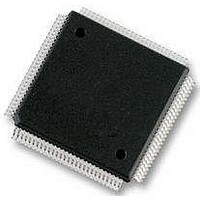
MC9S12E128CPV Freescale Semiconductor, MC9S12E128CPV Datasheet - Page 536

MC9S12E128CPV
Manufacturer Part Number
MC9S12E128CPV
Description
Microcontrollers (MCU) 16 Bit 16MHz
Manufacturer
Freescale Semiconductor
Datasheet
1.MC9S12E128CPV.pdf
(606 pages)
Specifications of MC9S12E128CPV
Data Bus Width
16 bit
Program Memory Type
Flash
Program Memory Size
128 KB
Data Ram Size
8 KB
Interface Type
SCI, SPI
Maximum Clock Frequency
25 MHz
Number Of Programmable I/os
92
Number Of Timers
16 bit
Operating Supply Voltage
3.135 V to 5.5 V
Maximum Operating Temperature
+ 85 C
Mounting Style
SMD/SMT
Package / Case
LQFP-112
Minimum Operating Temperature
- 40 C
On-chip Adc
10 bit
On-chip Dac
8 bit, 2 Channel
Lead Free Status / Rohs Status
No RoHS Version Available
Available stocks
Company
Part Number
Manufacturer
Quantity
Price
Company:
Part Number:
MC9S12E128CPVE
Manufacturer:
Freescale Semiconductor
Quantity:
10 000
- Current page: 536 of 606
- Download datasheet (4Mb)
Chapter 18 Multiplexed External Bus Interface (MEBIV3)
18.4
18.4.1
The external signals LSTRB, R/W, and AB0 indicate the type of bus access that is taking place. Accesses
to the internal RAM module are the only type of access that would produce LSTRB = AB0 = 1, because
the internal RAM is specifically designed to allow misaligned 16-bit accesses in a single cycle. In these
cases the data for the address that was accessed is on the low half of the data bus and the data for
address + 1 is on the high half of the data bus. This is summarized in
18.4.2
In order to allow fast internal bus cycles to coexist in a system with slower external memory resources, the
HCS12 supports the concept of stretched bus cycles (module timing reference clocks for timers and baud
rate generators are not affected by this stretching). Control bits in the MISC register in the MMC sub-block
of the core specify the amount of stretch (0, 1, 2, or 3 periods of the internal bus-rate clock). While
stretching, the CPU state machines are all held in their current state. At this point in the CPU bus cycle,
write data would already be driven onto the data bus so the length of time write data is valid is extended
in the case of a stretched bus cycle. Read data would not be captured by the system until the E clock falling
edge. In the case of a stretched bus cycle, read data is not required until the specified setup time before the
falling edge of the stretched E clock. The chip selects, and R/W signals remain valid during the period of
stretching (throughout the stretched E high time).
536
Functional Description
Detecting Access Type from External Signals
Stretched Bus Cycles
The address portion of the bus cycle is not stretched
LSTRB
1
0
1
0
0
1
0
1
Table 18-15. Access Type vs. Bus Control Pins
AB0
0
1
0
1
0
1
0
1
MC9S12E128 Data Sheet, Rev. 1.07
R/W
1
1
0
0
1
1
0
0
NOTE
8-bit read of an even address
8-bit read of an odd address
8-bit write of an even address
8-bit write of an odd address
16-bit read of an even address
16-bit read of an odd address
(low/high data swapped)
16-bit write to an even address
16-bit write to an odd address
(low/high data swapped)
Type of Access
.
Table
18-15.
Freescale Semiconductor
Related parts for MC9S12E128CPV
Image
Part Number
Description
Manufacturer
Datasheet
Request
R
Part Number:
Description:
Manufacturer:
Freescale Semiconductor, Inc
Datasheet:
Part Number:
Description:
Manufacturer:
Freescale Semiconductor, Inc
Datasheet:
Part Number:
Description:
Manufacturer:
Freescale Semiconductor, Inc
Datasheet:
Part Number:
Description:
Manufacturer:
Freescale Semiconductor, Inc
Datasheet:
Part Number:
Description:
Manufacturer:
Freescale Semiconductor, Inc
Datasheet:
Part Number:
Description:
Manufacturer:
Freescale Semiconductor, Inc
Datasheet:
Part Number:
Description:
Manufacturer:
Freescale Semiconductor, Inc
Datasheet:
Part Number:
Description:
Manufacturer:
Freescale Semiconductor, Inc
Datasheet:
Part Number:
Description:
Manufacturer:
Freescale Semiconductor, Inc
Datasheet:
Part Number:
Description:
Manufacturer:
Freescale Semiconductor, Inc
Datasheet:
Part Number:
Description:
Manufacturer:
Freescale Semiconductor, Inc
Datasheet:
Part Number:
Description:
Manufacturer:
Freescale Semiconductor, Inc
Datasheet:
Part Number:
Description:
Manufacturer:
Freescale Semiconductor, Inc
Datasheet:
Part Number:
Description:
Manufacturer:
Freescale Semiconductor, Inc
Datasheet:
Part Number:
Description:
Manufacturer:
Freescale Semiconductor, Inc
Datasheet:


