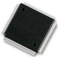
MC9S12E128CPV Freescale Semiconductor, MC9S12E128CPV Datasheet - Page 229

MC9S12E128CPV
Manufacturer Part Number
MC9S12E128CPV
Description
Microcontrollers (MCU) 16 Bit 16MHz
Manufacturer
Freescale Semiconductor
Datasheet
1.MC9S12E128CPV.pdf
(606 pages)
Specifications of MC9S12E128CPV
Data Bus Width
16 bit
Program Memory Type
Flash
Program Memory Size
128 KB
Data Ram Size
8 KB
Interface Type
SCI, SPI
Maximum Clock Frequency
25 MHz
Number Of Programmable I/os
92
Number Of Timers
16 bit
Operating Supply Voltage
3.135 V to 5.5 V
Maximum Operating Temperature
+ 85 C
Mounting Style
SMD/SMT
Package / Case
LQFP-112
Minimum Operating Temperature
- 40 C
On-chip Adc
10 bit
On-chip Dac
8 bit, 2 Channel
Lead Free Status / Rohs Status
No RoHS Version Available
Available stocks
Company
Part Number
Manufacturer
Quantity
Price
Company:
Part Number:
MC9S12E128CPVE
Manufacturer:
Freescale Semiconductor
Quantity:
10 000
- Current page: 229 of 606
- Download datasheet (4Mb)
6.3.2.16
The A/D conversion results are stored in 16 read-only result registers. The result data is formatted in the
result registers bases on two criteria. First there is left and right justification; this selection is made using
the DJM control bit in ATDCTL5. Second there is signed and unsigned data; this selection is made using
the DSGN control bit in ATDCTL5. Signed data is stored in 2’s complement format and only exists in left
justified format. Signed data selected for right justified format is ignored.
Read: Anytime
Write: Anytime in special mode, unimplemented in normal modes
6.3.2.16.1
Freescale Semiconductor
R (10-BIT)
R (10-BIT)
R (8-BIT)
R (8-BIT)
Reset
Reset
W
W
Figure 6-18. Left Justified, ATD Conversion Result Register x, High Byte (ATDDRxH)
Figure 6-19. Left Justified, ATD Conversion Result Register x, Low Byte (ATDDRxL)
BIT 9 MSB
BIT 7 MSB
ATD Conversion Result Registers (ATDDRx)
Left Justified Result Data
BIT 1
u
0
7
0
7
= Unimplemented or Reserved
= Unimplemented or Reserved
BIT 0
BIT 8
BIT 6
6
u
0
0
6
MC9S12E128 Data Sheet, Rev. 1.07
BIT 7
BIT 5
0
0
0
5
0
5
BIT 6
BIT 4
4
0
0
0
0
4
Chapter 6 Analog-to-Digital Converter (ATD10B16CV2)
BIT 5
BIT 3
0
0
0
3
0
3
u = Unaffected
BIT 4
BIT 2
2
0
0
0
0
2
BIT 3
BIT 1
0
0
0
1
0
1
BIT 2
BIT 0
0
0
0
0
0
0
229
Related parts for MC9S12E128CPV
Image
Part Number
Description
Manufacturer
Datasheet
Request
R
Part Number:
Description:
Manufacturer:
Freescale Semiconductor, Inc
Datasheet:
Part Number:
Description:
Manufacturer:
Freescale Semiconductor, Inc
Datasheet:
Part Number:
Description:
Manufacturer:
Freescale Semiconductor, Inc
Datasheet:
Part Number:
Description:
Manufacturer:
Freescale Semiconductor, Inc
Datasheet:
Part Number:
Description:
Manufacturer:
Freescale Semiconductor, Inc
Datasheet:
Part Number:
Description:
Manufacturer:
Freescale Semiconductor, Inc
Datasheet:
Part Number:
Description:
Manufacturer:
Freescale Semiconductor, Inc
Datasheet:
Part Number:
Description:
Manufacturer:
Freescale Semiconductor, Inc
Datasheet:
Part Number:
Description:
Manufacturer:
Freescale Semiconductor, Inc
Datasheet:
Part Number:
Description:
Manufacturer:
Freescale Semiconductor, Inc
Datasheet:
Part Number:
Description:
Manufacturer:
Freescale Semiconductor, Inc
Datasheet:
Part Number:
Description:
Manufacturer:
Freescale Semiconductor, Inc
Datasheet:
Part Number:
Description:
Manufacturer:
Freescale Semiconductor, Inc
Datasheet:
Part Number:
Description:
Manufacturer:
Freescale Semiconductor, Inc
Datasheet:
Part Number:
Description:
Manufacturer:
Freescale Semiconductor, Inc
Datasheet:


