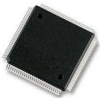
MC9S12E128CPV Freescale Semiconductor, MC9S12E128CPV Datasheet - Page 87

MC9S12E128CPV
Manufacturer Part Number
MC9S12E128CPV
Description
Microcontrollers (MCU) 16 Bit 16MHz
Manufacturer
Freescale Semiconductor
Datasheet
1.MC9S12E128CPV.pdf
(606 pages)
Specifications of MC9S12E128CPV
Data Bus Width
16 bit
Program Memory Type
Flash
Program Memory Size
128 KB
Data Ram Size
8 KB
Interface Type
SCI, SPI
Maximum Clock Frequency
25 MHz
Number Of Programmable I/os
92
Number Of Timers
16 bit
Operating Supply Voltage
3.135 V to 5.5 V
Maximum Operating Temperature
+ 85 C
Mounting Style
SMD/SMT
Package / Case
LQFP-112
Minimum Operating Temperature
- 40 C
On-chip Adc
10 bit
On-chip Dac
8 bit, 2 Channel
Lead Free Status / Rohs Status
No RoHS Version Available
Available stocks
Company
Part Number
Manufacturer
Quantity
Price
Company:
Part Number:
MC9S12E128CPVE
Manufacturer:
Freescale Semiconductor
Quantity:
10 000
- Current page: 87 of 606
- Download datasheet (4Mb)
2.3
This section describes the FTS128K1 memory map and registers.
2.3.1
The FTS128K1 memory map is shown in
addresses between 0x4000 and 0xFFFF, which corresponds to three 16 Kbyte pages. The content of the
HCS12 Core PPAGE register is used to map the logical middle page ranging from address 0x8000 to
0xBFFF to any physical 16K byte page in the Flash array memory.
2.3.2.5) can be set to globally protect the entire Flash array. Three separate areas, one starting from the
Flash array starting address (called lower) towards higher addresses, one growing downward from the
Flash array end address (called higher), and the remaining addresses, can be activated for protection. The
Flash array addresses covered by these protectable regions are shown in
area is mainly targeted to hold the boot loader code since it covers the vector space. The lower address area
can be used for EEPROM emulation in an MCU without an EEPROM module since it can be left
unprotected while the remaining addresses are protected from program or erase. Default protection
settings as well as security information that allows the MCU to restrict access to the Flash module are
stored in the Flash configuration field described in
1. By placing 0x3E/0x3F in the HCS12 Core PPAGE register, the bottom/top fixed 16 Kbyte pages can be seen twice in the MCU
Freescale Semiconductor
memory map.
0xFF08–0xFF0C
0xFF00–0xFF07
Memory Map and Registers
Flash Address
Module Memory Map
0xFF0D
0xFF0E
0xFF0F
(bytes)
Size
8
5
1
1
1
Table 2-1. Flash Configuration Field
Backdoor Key to unlock security
Reserved
Flash Protection byte
Refer to
Reserved
Flash Security/Options byte
Refer to
MC9S12E128 Data Sheet, Rev. 1.07
Figure
Section 2.3.2.5, “Flash Protection Register (FPROT)”
Section 2.3.2.2, “Flash Security Register (FSEC)”
2-2. The HCS12 architecture places the Flash array
Table
2-1.
Description
Chapter 2 128 Kbyte Flash Module (FTS128K1V1)
1
The FPROT register (see
Figure
2-2. The higher address
Section
87
Related parts for MC9S12E128CPV
Image
Part Number
Description
Manufacturer
Datasheet
Request
R
Part Number:
Description:
Manufacturer:
Freescale Semiconductor, Inc
Datasheet:
Part Number:
Description:
Manufacturer:
Freescale Semiconductor, Inc
Datasheet:
Part Number:
Description:
Manufacturer:
Freescale Semiconductor, Inc
Datasheet:
Part Number:
Description:
Manufacturer:
Freescale Semiconductor, Inc
Datasheet:
Part Number:
Description:
Manufacturer:
Freescale Semiconductor, Inc
Datasheet:
Part Number:
Description:
Manufacturer:
Freescale Semiconductor, Inc
Datasheet:
Part Number:
Description:
Manufacturer:
Freescale Semiconductor, Inc
Datasheet:
Part Number:
Description:
Manufacturer:
Freescale Semiconductor, Inc
Datasheet:
Part Number:
Description:
Manufacturer:
Freescale Semiconductor, Inc
Datasheet:
Part Number:
Description:
Manufacturer:
Freescale Semiconductor, Inc
Datasheet:
Part Number:
Description:
Manufacturer:
Freescale Semiconductor, Inc
Datasheet:
Part Number:
Description:
Manufacturer:
Freescale Semiconductor, Inc
Datasheet:
Part Number:
Description:
Manufacturer:
Freescale Semiconductor, Inc
Datasheet:
Part Number:
Description:
Manufacturer:
Freescale Semiconductor, Inc
Datasheet:
Part Number:
Description:
Manufacturer:
Freescale Semiconductor, Inc
Datasheet:


