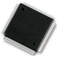
MC9S12E128CPV Freescale Semiconductor, MC9S12E128CPV Datasheet - Page 338

MC9S12E128CPV
Manufacturer Part Number
MC9S12E128CPV
Description
Microcontrollers (MCU) 16 Bit 16MHz
Manufacturer
Freescale Semiconductor
Datasheet
1.MC9S12E128CPV.pdf
(606 pages)
Specifications of MC9S12E128CPV
Data Bus Width
16 bit
Program Memory Type
Flash
Program Memory Size
128 KB
Data Ram Size
8 KB
Interface Type
SCI, SPI
Maximum Clock Frequency
25 MHz
Number Of Programmable I/os
92
Number Of Timers
16 bit
Operating Supply Voltage
3.135 V to 5.5 V
Maximum Operating Temperature
+ 85 C
Mounting Style
SMD/SMT
Package / Case
LQFP-112
Minimum Operating Temperature
- 40 C
On-chip Adc
10 bit
On-chip Dac
8 bit, 2 Channel
Lead Free Status / Rohs Status
No RoHS Version Available
Available stocks
Company
Part Number
Manufacturer
Quantity
Price
Company:
Part Number:
MC9S12E128CPVE
Manufacturer:
Freescale Semiconductor
Quantity:
10 000
- Current page: 338 of 606
- Download datasheet (4Mb)
Chapter 11 Pulse Width Modulator with Fault Protection (PMF15B6CV2)
11.3.2.10 PMF Output Control Register (PMFOUTC)
Read and write anytime.
338
OUTCTL[5:0]
Module Base + 0x000C
Reset
Field
5–0
W
R
PMF Output Control Bits — These bits enable software control of their corresponding PWM pin. When
OUTCTLx is set, the OUTx bit activates and deactivates the PWMx output.
When operating the PWM in complementary mode, these bits must be switched in pairs for proper operation.
That is OUTCTL0 and OUTCTL1 must have the same value; OUTCTL2 and OUTCTL3 must have the same
value; and OUTCTL4 and OUTCTL5 must have the same value.
0 Software control disabled
1 Software control enabled
where X is 0, 1, 2, 3, 4 and 5
0
0
7
Fault2
Fault0
Fault1
Fault3
= Unimplemented or Reserved
DMPx3
Figure 11-16. PMF Output Control Register (PMFOUTC)
0
0
6
PWM Pin
DMPx2
PWM0
PWM1
PWM2
PWM3
PWM4
PWM5
Table 11-13. PMFOUTC Field Descriptions
OUTCTL5
DMPx1
MC9S12E128 Data Sheet, Rev. 1.07
0
5
Figure 11-15. Fault Decoder
Table 11-12. Fault Mapping
DMPx0
OUTCTL4
0
4
Controlling Register Bits
Description
DMP53
DMP03
DMP13
DMP23
DMP33
DMP43
OUTCTL3
–
–
–
–
–
–
0
3
DMP00
DMP10
DMP20
DMP30
DMP40
DMP50
where X is 0, 1, 2, 3, 4, 5
OUTCTL2
DISABLE PWM PIN x
0
2
OUTCTL1
Freescale Semiconductor
0
1
OUTCTL0
0
0
Related parts for MC9S12E128CPV
Image
Part Number
Description
Manufacturer
Datasheet
Request
R
Part Number:
Description:
Manufacturer:
Freescale Semiconductor, Inc
Datasheet:
Part Number:
Description:
Manufacturer:
Freescale Semiconductor, Inc
Datasheet:
Part Number:
Description:
Manufacturer:
Freescale Semiconductor, Inc
Datasheet:
Part Number:
Description:
Manufacturer:
Freescale Semiconductor, Inc
Datasheet:
Part Number:
Description:
Manufacturer:
Freescale Semiconductor, Inc
Datasheet:
Part Number:
Description:
Manufacturer:
Freescale Semiconductor, Inc
Datasheet:
Part Number:
Description:
Manufacturer:
Freescale Semiconductor, Inc
Datasheet:
Part Number:
Description:
Manufacturer:
Freescale Semiconductor, Inc
Datasheet:
Part Number:
Description:
Manufacturer:
Freescale Semiconductor, Inc
Datasheet:
Part Number:
Description:
Manufacturer:
Freescale Semiconductor, Inc
Datasheet:
Part Number:
Description:
Manufacturer:
Freescale Semiconductor, Inc
Datasheet:
Part Number:
Description:
Manufacturer:
Freescale Semiconductor, Inc
Datasheet:
Part Number:
Description:
Manufacturer:
Freescale Semiconductor, Inc
Datasheet:
Part Number:
Description:
Manufacturer:
Freescale Semiconductor, Inc
Datasheet:
Part Number:
Description:
Manufacturer:
Freescale Semiconductor, Inc
Datasheet:


